Create a LabVIEW FPGA Project and VI
The simulation example will compare an Add function executing in a normal versus a single-cycle timed loop in a LabVIEW FPGA VI.
First, create a new LabVIEW FPGA project and an FPGA VI to test in ISim.
Note: If you use the attached lv_fpga_isim_ex project files, you can skip this section.
-
Create a LabVIEW project and save the project as LV FPGA ISim Example.lvproj.
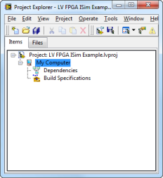
Figure 1. Create a LabVIEW Project
- Add an FPGA target to the project. The target should support LabVIEW FPGA simulation. For this example, use an NI PXI-7854R R Series Multifunction RIO device.
Note: Support for cycle-accurate simulation varies by FPGA target. Refer to the target hardware documentation for information about simulation support. -
Add a new VI under the PXI-7854R target and name the VI FPGA Add Test.vi.
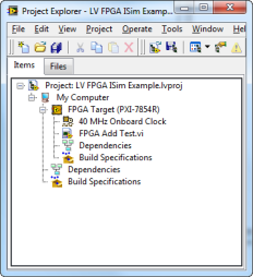
Figure 2. Add the FPGA target and a New VI
- This VI benchmarks the execution time difference between using an Add function in a normal while loop versus a single-cycle timed loop (SCTL).
As show in Figure 3 below, each loop contains an Add function and an indicator. A sequence structure encapsulates the loops in order to control when the loop execution starts, and the start Boolean triggers the test. Since the simulation also accounts for communication delays between the LabVIEW host interface and the FPGA, the start delay also ensures that in the simulation the written data has been loaded on the registers before the Add functions are allowed to execute.
Note: The completed VI is available in the attached lv_fpga_isim_ex files.
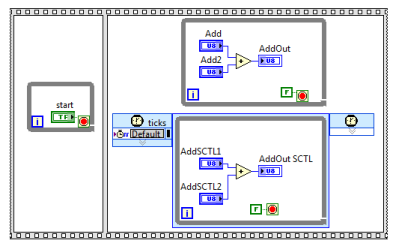
Figure 3. Create a VI to benchmark the execution of the Add function in different loop types
Configure the LabVIEW FPGA Module for Simulation
Before you build a simulation export, you need to configure LabVIEW to export to ISim.
- In LabVIEW, select Tools»Options to display the Options dialog box, then select FPGA Module from the Category list.
-
From the Simulator pull-down menu, select ISim.
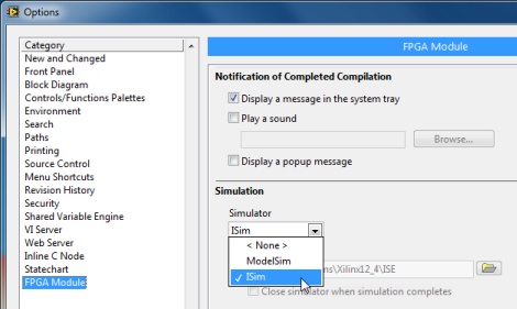
Figure 4. Configure LabVIEW to Export Simulation Files to ISim
- To configure the execution mode of the FPGA target. Right-click on the PXI-7854R target in the Project Explorer window and select Execute VI On»Third-Party Simulator.
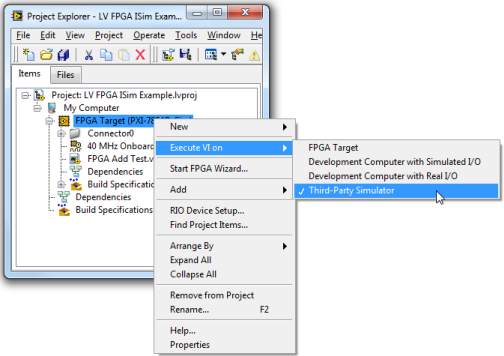
Figure 5. Select the Third-Party Simulator Execution Mode for the FPGA Target
Create and Build Simulation Exports
Next you will generate the simulation export files, including the VHDL test bench, which you will modify and then use to execute a simulation in ISim.
- Create a simulation export build specification under FPGA Target.
To create the build specification, right-click Build Specifications under FPGA Target and select New»Simulation Export.
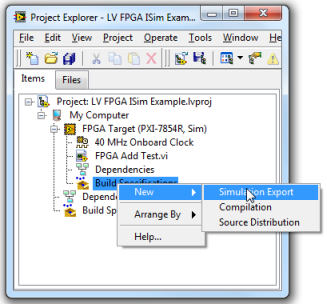
Figure 6. Create a Simulation Export Build Specification
-
In the dialog box that appears, set the top-level VI to simulate by navigating to the Source Files tab and selecting FPGA Add Test.vi. On this tab you can specify different signals that will be automatically added to the simulation waveform. For this example leave these as the default value.
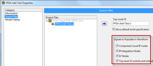
Figure 7. In the Source Files Tab Select the VI to Simulate and the Signals to Expose in the Simulator
-
Go back to the Information page and see that the build specification name has changed to “FPGA Add Test” to match the name of your VI. Also in the Information tab you can also set the top-level simulation model name and Destination directory. The top-level simulation model name is the name of the VHDL file that will be generated for the VI. For this example leave this field as the default value.
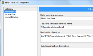
Figure 8. Confirm that VI Name and Build Specification Name Match
-
Click Build to save the build specification and generate the testbench files. You should see a dialog window indicating when the simulation export has been successfully built. Click Done in that dialog window.
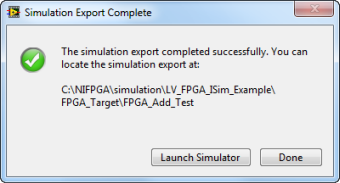
Figure 9. Simulation Dialog Window
-
Right-click the build specification and select Explore to navigate to the generated simulation files.
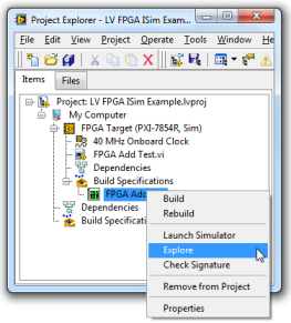
Figure 10. Right-click on the Build Specification to Explore Simulation Export Directory
- Review the content of the folders generated in the simulation export directory:
- isim - This folder contains files used by the ISim simulation tool. You do not need to view or edit any files in this folder.
- niFpga - The niFPGA folder contains VHDL files generated by the LabVIEW FPGA Module to implement the simulation model. These files are regenerated each time the simulation export is built and should not be modified. However, some of these files can be useful later in the application.
- user - This directory contains files that you can edit, including the top-level test bench files. The first time the build specification is built the test benches templates are generated. A copy of the templates is generated on each build in the niFpga directory for reference. The test bench files are described in more detail in the next section of this tutorial.
Develop a Test Bench and Simulate the VI
Before running the ISim tool, you need to modify the template VHDL test bench exported by LabVIEW FPGA to exercise your logic appropriately.
-
Picking up from the last section, navigate to the user directory and open the test bench file named tb_NiFpgaSimulationModel.vhd. Scan through the VHDL template that LabVIEW created as the foundation for your test bench. Notice that the architecture block contains a block named MainStimulusBlock and an instantiation of the NiFpgaSimulationModel component.
MainStimulusBlock contains the host interface code. The existing code performs a download, open, run, and then close. In the next step we will add write and read operations to exercise the design. Notice that the paradigm is similar to that used if you were going to develop the test bench in a LabVIEW host VI.
NiFpgaSimulationModel implements the VI simulation model. You should not have to modify this instantiation.
- Test your Add function benchmark VI by writing values to the four input controls for the two Add functions and then reading the two Add output indicators. To gate the test you will also write to the start Boolean to determine when the benchmark should start. To do these writes and reads, use the NiFpga_Write and NiFpga_Read procedures.
Look up the definitions of these procedures in one of the VHDL packages in the niFpga directory. You should be familiar with these packages:
- PkgNiFpgaSimControlAndIndicatorProcedures.vhd contains control/indicator read/write procedure definitions.
- PkgNiFpgaSimFifoProcedures.vhd contains FIFO method definitions, such as reading, writing, starting, and stopping FIFOs.
- PkgNiFpgaSimMiscProcedures.vhd contains the other host interface procedure definitions, such as open, download, close, run, and reset.
Because this example uses control/indicator procedures, look in PkgNiFpgaSimControlAndIndicatorProcedures.vhd. Since your control and indicator are U8 types, you need the NiFpga_Read and NiFpga_Write versions that use unsigned data types. There are overloaded versions of these functions for unsigned, Boolean, and tFxpGen (for fixed-point types).

Figure 11. Find the FPGA Write and Read Definitions in the PkgNiFpgaSimControlAndIndicatorProcedures file.
- Add five NiFpga_Write and two NiFpga_Read before the call to NiFpga_Close in the test bench file, as shown below. You will fill in the parameters in the next step.
        --  This is an example of how to write a control:

        --  NiFpga_Write (

        --    Address => <constant in PkgRegister k[ControlName]_ctl_X>,

        --    Data => <variable [ControlName]_ctl_X_Data>,

        --    FiClock => FiClock,

        --    fiHostToTargetInterface => fiHostToTargetInterface,

        --    fiHostToTargetReady => fiHostToTargetReady,

        --    fiErrorStatusIn => fiErrorStatus,

        --    fiErrorStatusOut => fiErrorStatus);

        --*********************************************************************

                                -- Write Host Variables to FPGA Registers

                                NiFpga_Write (

           Address => ,

           Data => ,

           FiClock => FiClock,

           fiHostToTargetInterface => fiHostToTargetInterface,

           fiHostToTargetReady => fiHostToTargetReady,

           fiErrorStatusIn => fiErrorStatus,

           fiErrorStatusOut => fiErrorStatus);


                                NiFpga_Write (

           Address =>,

           Data =>,

           FiClock => FiClock,

           fiHostToTargetInterface => fiHostToTargetInterface,

           fiHostToTargetReady => fiHostToTargetReady,

           fiErrorStatusIn => fiErrorStatus,

           fiErrorStatusOut => fiErrorStatus);


                                -- Assert the Start Boolean to Begin Execution of Loops

                                NiFpga_Write (

           Address =>,

           Data =>,

           FiClock => FiClock,

           fiHostToTargetInterface => fiHostToTargetInterface,

           fiHostToTargetReady => fiHostToTargetReady,

           fiErrorStatusIn => fiErrorStatus,

           fiErrorStatusOut => fiErrorStatus);


                                -- Read the Add Outputs from Normal and Single-Cycle Timed Loops

         NiFpga_Read (

           Address =>,

           Data =>,

           FiClock => FiClock,

           fiHostToTargetInterface => fiHostToTargetInterface,

           fiTargetToHostInterface => fiTargetToHostInterface,

           fiHostToTargetReady => fiHostToTargetReady,

           fiTargetToHostReady =>  fiTargetToHostReady,

           fiErrorStatusIn => fiErrorStatus,

           fiErrorStatusOut => fiErrorStatus);
- To fill in the address parameter, find the constants for control/indicator addresses in the /niFpga/PkgRegister.vhd file. Open this file to find the following constants for control and indicator:
kAdd1_ctl_0
kAdd2_ctl_1
kAddSCTL1_ctl_4
kAddSCTL2_ctl_5
kstart_ctl_6
kAddOut_ind_2
kAddOut_SCTL_ind_3
Fill these in as the address parameter in the procedure calls.
- To fill in the data parameter, use tU8 type variables, since the control and indicator are U8. (Find these data-type definitions in the /niFpga/PkgNiFpgaSimInterfaceLvDataTypes.vhd file.) If you look at the beginning of the MainStimulusProcess statement, you can see that there are variables already defined.
     MainStimulusProcess:process

      variable fiErrorStatus : tErrorStatus := (Status => false, Code => 0);

        --=====================================================================

        --Control and Indicator Data Variables

        -----------------------------------------------------------------------

        -- Use these variables with the NiFpga_Write and NiFpga_Read commands

        -- for controls and indicators to guarantee the correct data type read

        -- or write operation is performed. Refer to the auto-generated

        -- file, PkgRegister.vhd, in the nifpga directory for the register

        -- offsets for the controls and indicators.

        -----------------------------------------------------------------------

        variable Add1_ctl_0_Data: tU8;

        variable Add2_ctl_1_Data: tU8;

        variable AddOut_ind_2_Data: tU8;

        variable AddOut_SCTL_ind_3_Data: tU8;

        variable AddSCTL1_ctl_4_Data: tU8;

        variable AddSCTL2_ctl_5_Data: tU8;

        variable start_ctl_6_Data: boolean;

        --=====================================================================
- Note that the other parameters that begin with fi* to standard signals are already connected within the test bench. These communicate with the testbench framework defined in the simulation model. You only need to be familiar with ErrorStatus signals. Monitor the signal fiErrorStatus in ISim for warnings and errors.
- Once you have filled in these parameters, the read and write procedures should look like this:
            -- Write Host Variables to FPGA Registers

              NiFpga_Write (

           Address => kAdd1_ctl_0,

           Data => Add1_ctl_0_Data,

           FiClock => FiClock,

           fiHostToTargetInterface => fiHostToTargetInterface,

           fiHostToTargetReady => fiHostToTargetReady,

           fiErrorStatusIn => fiErrorStatus,

           fiErrorStatusOut => fiErrorStatus);


              NiFpga_Write (

           Address => kAdd2_ctl_1,

           Data => Add2_ctl_1_Data,

           FiClock => FiClock,

           fiHostToTargetInterface => fiHostToTargetInterface,

           fiHostToTargetReady => fiHostToTargetReady,

           fiErrorStatusIn => fiErrorStatus,

           fiErrorStatusOut => fiErrorStatus);


              NiFpga_Write (

           Address => kAddSCTL1_ctl_4,

           Data => AddSCTL1_ctl_4_Data,

           FiClock => FiClock,

           fiHostToTargetInterface => fiHostToTargetInterface,

           fiHostToTargetReady => fiHostToTargetReady,

           fiErrorStatusIn => fiErrorStatus,

           fiErrorStatusOut => fiErrorStatus);


              NiFpga_Write (

           Address => kAddSCTL2_ctl_5,

           Data => AddSCTL2_ctl_5_Data,

           FiClock => FiClock,

           fiHostToTargetInterface => fiHostToTargetInterface,

           fiHostToTargetReady => fiHostToTargetReady,

           fiErrorStatusIn => fiErrorStatus,

           fiErrorStatusOut => fiErrorStatus);


              -- Assert the Start Boolean to Begin Execution of Loops

              NiFpga_Write (

           Address => kstart_ctl_6,

           Data => start_ctl_6_Data,

           FiClock => FiClock,

           fiHostToTargetInterface => fiHostToTargetInterface,

           fiHostToTargetReady => fiHostToTargetReady,

           fiErrorStatusIn => fiErrorStatus,

           fiErrorStatusOut => fiErrorStatus);


              -- Read the Add Outputs from Normal and Single-Cycle Timed Loops

         NiFpga_Read (

           Address => kAddOut_ind_2,

           Data => AddOut_ind_2_Data,

           FiClock => FiClock,

           fiHostToTargetInterface => fiHostToTargetInterface,

           fiTargetToHostInterface => fiTargetToHostInterface,

           fiHostToTargetReady => fiHostToTargetReady,

           fiTargetToHostReady =>  fiTargetToHostReady,

           fiErrorStatusIn => fiErrorStatus,

           fiErrorStatusOut => fiErrorStatus);


         NiFpga_Read (

           Address => kAddOut_SCTL_ind_3,

           Data => AddOut_SCTL_ind_3_Data,

           FiClock => FiClock,

           fiHostToTargetInterface => fiHostToTargetInterface,

           fiTargetToHostInterface => fiTargetToHostInterface,

           fiHostToTargetReady => fiHostToTargetReady,

           fiTargetToHostReady =>  fiTargetToHostReady,

           fiErrorStatusIn => fiErrorStatus,

           fiErrorStatusOut => fiErrorStatus);
- Now, set the AddSCTL1_ctl_4_Data, AddSCTL2_ctl_5_Data, Add1_ctl_0_Data, Add2_ctl_1_Data, and start_ctl_6_Data variable value before writing it to the control. Insert the following line before the call to NiFpga_Write:
              -- Initialize the Host Variables to Test Values

              AddSCTL1_ctl_4_Data := to_unsigned(1, AddSCTL1_ctl_4_Data'length);

              AddSCTL2_ctl_5_Data := to_unsigned(2, AddSCTL2_ctl_5_Data'length);

              Add1_ctl_0_Data := to_unsigned(4, Add1_ctl_0_Data'length);

              Add2_ctl_1_Data := to_unsigned(3, Add2_ctl_1_Data'length);

              start_ctl_6_Data := true;

              -- Write Host Variables to FPGA Registers

              NiFpga_Write (
- You are now ready to simulate. Make sure that you have saved the tb_NiFpgaSimulationModel.vhd file. Then compile and launch ISim by double-clicking the RegenerateISim batch file in the user directory. This brings up the ISim tool with the FPGA Add Test project already loaded.
- You can now run the testbench by selecting Simulation»Run All or use the F5 shortcut.

Figure 12. Execute the ISim simulation by navigating to Simulation»RunAll
- Now, examine the waveform signals. Zoom out to full by selecting View»Zoom»To Full View so that you can see the entire waveform. Then, expand the “start”, “AddOut SCTL” and “AddOut” headings in the waveform to see detailed information on the control and indicator.
 Figure 13
. Examine the Waveform Signals
Note: There are several items under your controls and indicators. Clock is the clock signal that the registers implementing the control/indicator are synchronous to. Data is the register value for the control/indicator. For example in this waveform the start value begins with a default value of 0, gets set to 1, and then returns to the default value of 0
- To learn more about the start signals during the short period of time after the start is asserted zoom in on this section of the simulation. Move the cursor to this area of interest and then select View»Zoom»To Cursors and then zoom in multiple times by clicking F8.
- By using Add markers and the Next Transition shortcuts available on the toolbar you can estimate that the Add function in the single-cycle timed loop takes about 75 nS to execute, whereas the Add function in the normal loop takes 150 nS to execute.
 Figure 14
. Using the create marker and next transition operations you can estimate the execution time for the Add functions.
Conclusion
The Xilinx ISim cycle-accurate simulator that is installed with the LabVIEW FPGA module provides a cost-effective means to validate your FPGA applications before deployment and without the time intensive compilation process. This tutorial stepped through the process of generating the LabVIEW FPGA simulation exports, developing a VHDL testbench, and executing the timing simulation in ISim. As shown in the tutorial, the simulator requires you to modify the VHDL testbench template generated by LabVIEW to exercise the application logic and as a result you should be familiar with HDL simulators and VHDL.