Introduction to the PXI Architecture
Contents
- Overview
- Hardware Overview
- Mechanical Architecture
- Electrical Architecture
- Software Overview
- Real-World Example: Communication Within a PXI System
- Next Steps
Overview
PXI systems provide high-performance modular instruments and other I/O modules with specialized synchronization and key software features for test and measurement applications from device validation to automated production test. For a high-level understanding of PXI, see the two images in Figure 1 that compare a PXI system’s chassis, controller, and PXI(e) peripheral modules to components of a commercial desktop PC. The key is to realize how PXI builds off of and maps to commercial PC technology:
- The PXI chassis compares to the desktop’s enclosure
- The PXI controller compares to the desktop’s CPU, memory, and I/O
- The PXI(e) peripheral modules compare to the desktop’s PCI(e) peripheral modules
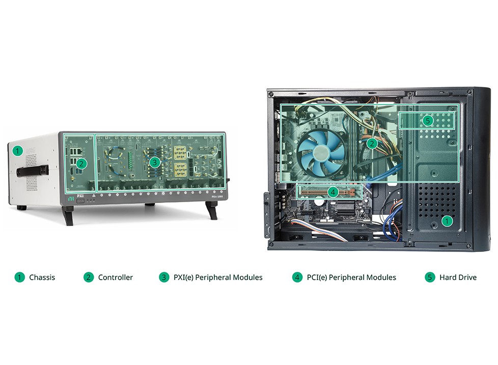
Figure 1: Compare a PXI system to a commercial desktop PC.
PXI (PCI eXtensions for Instrumentation) is a proven PC-based platform for measurement and automation systems. It provides power, cooling, and a communication bus to support multiple instrumentation modules within the same enclosure. PXI uses commercial PC-based PCI bus technology while combining rugged CompactPCI modular packaging, as well as key timing and synchronization features.
Peripheral Component Interconnect Special Interest Group (PCI-SIG) significantly improved system bandwidth when they released the evolution of PCI with the PCI Express standard. The PXI Systems Alliance (PXISA), which governs PXI, adopted the latest generation of commercial PC bus technology to evolve PXI to PXI Express. PXI Express maintains PXI features to ensure backward compatibility while providing more bandwidth, power, cooling, and timing and synchronization features in addition to the standard PXI features.
PXI and PXI Express may seem complex with so many features, however, these technologies have a common core: mainstream PC communication buses. PXI and PXI Express chassis provide a well-known, familiar architecture for today’s engineer’s measurement and automation system.
Because PXI is an open specification that is managed by the PXISA, any vendor can build PXI products. To help explain the low-level details of a PXI system, this white paper highlights the specification defined by the PXISA and how it is implemented on NI PXI hardware.
Hardware Overview
The PXISA hardware specification stipulates all feature requirements pertaining to the mechanical, electrical, and software architectures. The PXI Express specification is an implementation of the CompactPCI and CompactPCI Express specifications. Figure 2 shows how the mechanical and electrical aspects combine the CompactPCI and CompactPCI Express specifications with key PXI features to create the overall architecture. Subsequent sections in this paper break down these hierarchies to go into each section in additional detail and explain how they specifically apply to PXI.
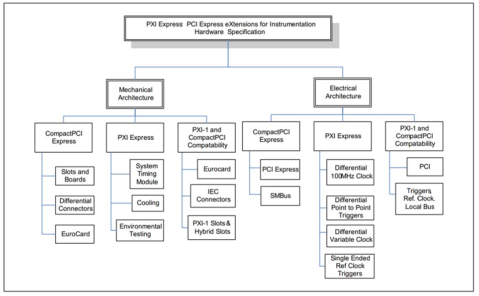
Figure 2: Overall PXI Architecture
Mechanical Architecture
The mechanical architecture specifies the physical compatibility between CompactPCI, CompactPCI Express, PXI, and PXI Express. For example, through the mechanical architecture, the system controller is defined to be in the leftmost slot of a PXI chassis to ensure it is at the left end of the PCI bus segment. It simplifies the integration and increases the degree of compatibility between chassis and controller options with this defined location.
The controller used in a PXI system could be an external PC or an embedded controller. Embedded controllers include standard features such as an integrated CPU, hard drive, memory, Ethernet, video, serial, USB, and other I/O peripherals. You can develop an application within a standard Windows environment—the same standard OS as an external PC.
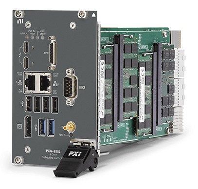
Figure 3: Embedded controllers feature a variety of I/O connectivity to interface to stand-alone instruments or peripheral devices.
The PXI specification adopts the high-performance IEC connectors and rugged EuroCard packaging system used by CompactPCI and CompactPCI Express.
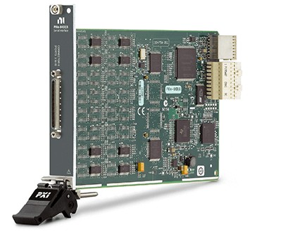
Figure 4: The NI PXI-8430 features EuroCard-like packaging and high-performance IEC connectors.
Through this connector the instrument connects and communicates with the rest of the system via the backplane's bus; for example, the PCI and PCI Express bus. These connector configurations maintain backward compatibility as the specification evolves to include the latest communication buses. More on this in the electrical section.
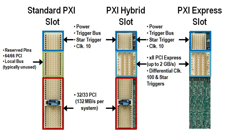
Figure 5: The specifications define the connector that is used for the communication to the PXI chassis.
The PXI mechanical specification also includes specific cooling and environmental improvements beyond CompactPCI and CompactPCI Express to ensure full operation in industrial environments.
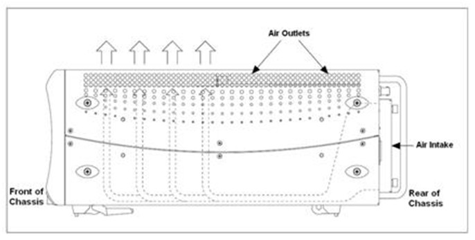
Figure 6: See how a PXI chassis aligns to the cooling requirements within the specification.
Electrical Architecture
The electrical architecture specifies the adherence to the PCI, PCI Express, CompactPCI, and CompactPCI Express specifications and power requirements. It also adds specific timing and synchronization features that make the PXI platform unique and suitable for high-performance test and measurement.
The core electrical feature of a PXI chassis is the communication bus. As PCI evolved into PCI Express, the specification has also evolved to ensure PXI can meet even more application needs by integrating PCI Express into the PXI chassis backplane.
For legacy instruments, PXI supports PCI communication—a 32-bit bus commonly used for transmitting and receiving data in parallel. The maximum bandwidth or throughput of a PCI instrument is 132 MB/s. As applications required higher bandwidth, PCI Express was defined where data is sent serially through pairs of transmit and receive connections called lanes, which give data the ability transfer at 250 MB/s per direction. This serial connection is known as a PCI Express Gen1 x1 “link” (by-one). Multiple lanes can be grouped together to form x2, x4, x8, x16, and x32 links to increase bandwidth. These links form a connection between a controller and a slot where an instrument is seated. For example, a x16 slot could transmit and receive 4 GB/s (250 MB/s * 16). To ensure compatibility with previous PXI instruments and new PXI Express instruments, both the PCI and PCI Express communication buses are incorporated into a PXI chassis. As the PCI Express specification evolves to the next generation, PXI will continue to incorporate the new capabilities into a PXI chassis while maintaining backward compatibility.
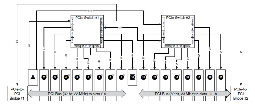
Figure 7: This example of the NI PXIe-1085 chassis highlights the PCI and PCI Express lines routing to each slot depending on the type of module that the slot accepts.
Along with the chassis communication buses evolving to incorporate the latest PC technology, PXI peripheral modules have evolved from PXI to PXI Express to take advantage of the PCI Express communication bus capabilities. To ensure module compatibility between PXI and PXI Express modules, the PXI specification added the hybrid slot. This slot gives you the ability to insert PXI or PXI Express peripheral modules in PXI chassis. A PXI chassis can include the following:
- A system slot, which accepts an embedded or remote PXI Express controller
- PXI peripheral slots, which accept PXI modules
- PXI Express hybrid peripheral slots, which accept PXI Express peripheral modules, 32-bit CompactPCI peripheral modules, and hybrid-compatible PXI peripheral modules
- A system timing slot, which accepts both PXI Express peripheral modules and PXI Express system timing modules
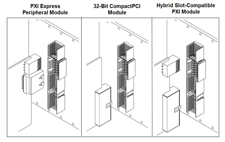
Figure 8: Slot Types That You Can Find Within a PXI Chassis
To bring it all together, the specification defines the technology that is available through the PXI chassis backplane.
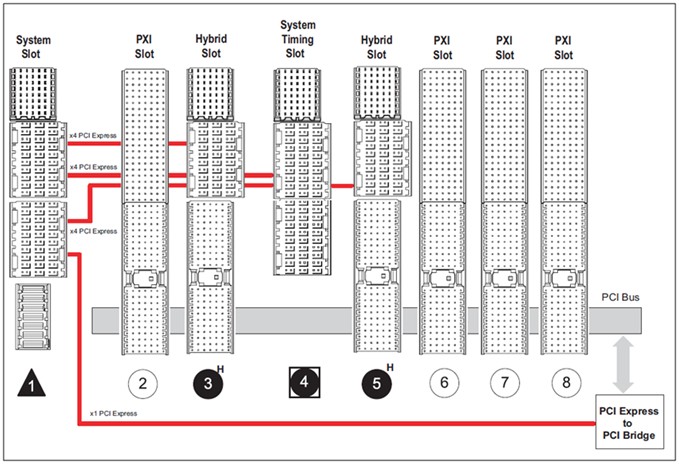
Figure 9: A PXI chassis incorporates the latest communication buses while routing to a variety of slot options to accommodate the requirements of a peripheral module.
In addition to the communication buses, the electrical specification also defines the timing and synchronization capabilities. It includes the definition of the PXI 10 MHz system clock, which is distributed to all peripheral modules in a system. This common reference clock can be used to synchronize multiple modules in a measurement or control system. In addition to clocking are PXI’s trigger capabilities such as a multidrop trigger bus and a matched trace length star trigger network. Eight PXI trigger lines form the PXI trigger bus, which is flexible and can be used in a variety of ways. For example, triggers can be used to synchronize the operation of several PXI peripheral modules.
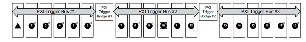
Figure 10: The NI PXIe-1085 chassis PXI trigger bus connectivity diagram shows how to pass triggers to the PXI peripheral modules.
For applications that require higher performance, the specification defines the PXI star trigger network, which adds a higher performance synchronization feature set to the PXI system. The star trigger network implements a dedicated trigger line between the system timing slot (denoted by a diamond or square glyph surrounding the slot number, PXI and PXI Express, respectively) and the other peripheral slots. A timing and synchronization module—a star trigger controller—is installed in this slot to provide precise clocks and trigger signals to other peripheral modules. It can also override the PXI chassis’ onboard VCXO accuracy with its onboard (TCXO, OCXO), derived (DDS), or external (rubidium source) clock to define the chassis’ high-frequency system reference clock, 10 MHz and 100 MHz clocks.
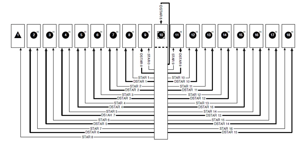
Figure 11: The NI PXIe-1085 chassis uses this star connectivity diagram to ensure the propagation delay is matched among each slot.
Below you can see how the PXI trigger bus and PXI star trigger network are routed between the slots. To ensure compatibility between all of these features, the SYNC 100 was introduced to synchronize the 10 MHz and the 100 MHz clocks within a chassis.
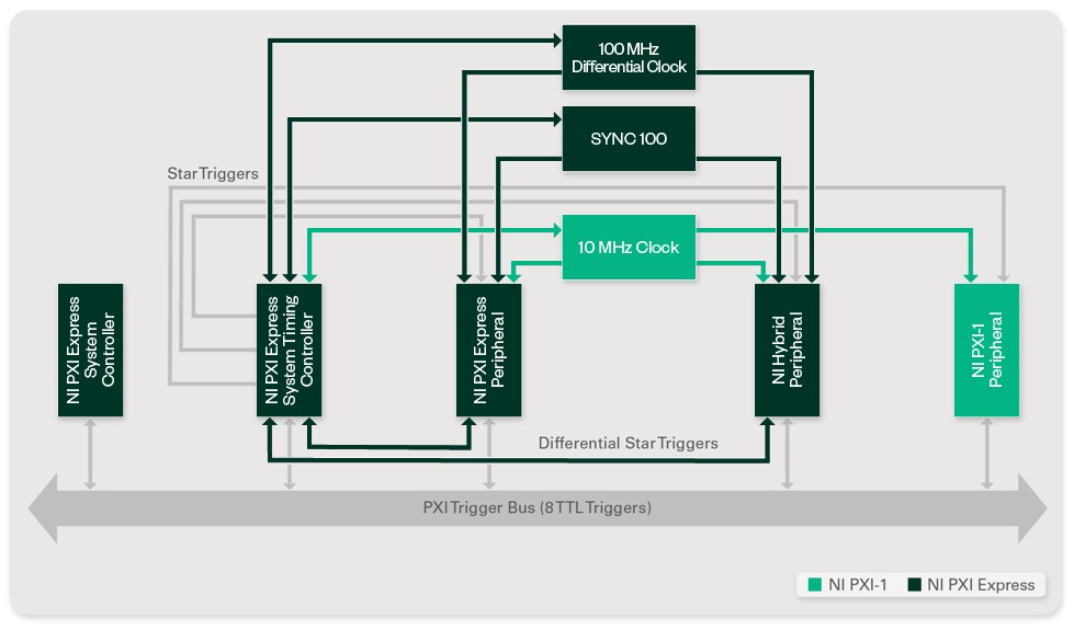
Figure 12: Choose the most appropriate configuration to ensure the timing and synchronization capabilities fit your application needs.
Software Overview
The PXI software specification defines the software architecture, a key element of the PXI platform. Because PXI is based on a software-defined instrumentation paradigm, PXI does not natively include direct user accessible features, such as a display screen, knobs, and push buttons, on the hardware. All the user accessible features are in software. The software frameworks define PXI system software requirements for both system controller modules and PXI peripheral modules. System controller modules and PXI peripheral modules have to meet certain requirements for OS and tool support to be considered compliant with a given PXI software framework.
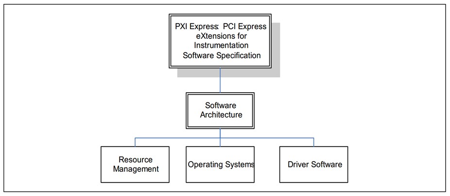
Figure 13: PXI Software Architecture
The PXI specification presents software frameworks for PXI systems based on Microsoft Windows OSs. As a result, the controller can use industry-standard application programming interfaces, such as NI LabVIEW, NI Measurement Studio, Visual Basic, and Visual C/C++, and Python. PXI also requires certain software components to be made available by module and chassis vendors. Initialization files that define system configuration and system capabilities are required for PXI components. Finally, implementation of the VISA, which has been widely adopted in the instrumentation field, is specified by PXI for configuration and control of VXI, GPIB, serial, and PXI instrumentation.
Figure 14: This diagram shows the complete PXI architecture when considering software’s role.
Real-World Example: Communication Within a PXI System
Consider a simple use case for a PXI system: generating a signal using a PXI module such as NI PXIe-5433. You use a Windows-based controller and write a program using LabVIEW software. LabVIEW communicates to the instrument via the instrument driver. Measurement & Automation Explorer (MAX) is used to ensure the system is set up for this communication.
Figure 15: Hardware Setup and Example of the Software Environment
To start the communication, you run a program written within LabVIEW. The LabVIEW program executes a sequence of operations, which take place behind the scenes. See the following walkthrough of the communication steps:
Step 1: LabVIEW running on a PXI system controller
The application code is compiled and converted into machine-level code.
Step 2: PXI system controller passes the set of commands written in LabVIEW to the instrument placed into a PXI peripheral slot
Within the PXI system controller memory and processor, the machine-level code converts to electrical signals and is passed along the PCI or PCI Express communication bus. In this example, it is the PCI Express communication that runs along the PXI chassis backplane connecting the system controller to the peripheral instrument.
Step 3: The commands are passed along the communication bus on the chassis backplane
The signal propagates through the PCI Express communication bus to the PXI slot where the instrument is seated.
Step 4: The code is passed to the instrument
The PXI module reads the sent commands. For this example, the NI PXIe-5433 generates a signal so the instrument reads the signal using circuitry on the module to perform the required action and generate a signal and pass it to the connector on the front of the module.
Figure 16 demonstrates how the communication is passed from the controller to the actual slot.
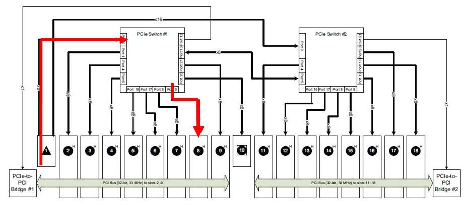
Figure 16: Example of Signal Propagation Through Backplane
Next Steps
- Explore PXI products for your test system
- Use the free NI PXI advisor to create your system today
- Review practical guides that outline how to build your test system
- For an example of how to get started using a PXI Express NI data acquisition device, visit Getting Started with PXI Express Multifunction I/O Hardware and LabVIEW.