Field Wiring and Noise Considerations for Analog Signals
Overview
Contents
- Types of Signal Sources and Measurement Systems
- Measuring Grounded Signal Sources
- Measuring Floating (Nonreferenced) Sources
- Minimizing Noise Coupling in the Interconnects
- Balanced Systems
- Solving Noise Problems in Measurement Setups
- Signal Processing Techniques for Noise Reduction
- References
- Learn More
Types of Signal Sources and Measurement Systems
By far the most common electrical equivalent produced by signal conditioning circuitry associated with sensors is in the form of voltage. Transformation to other electrical phenomena such as current and frequency may be encountered in cases where the signal is to be carried over long cabling in harsh environments. Since in virtually all cases the transformed signal is ultimately converted back into a voltage signal before measurement, it is important to understand the voltage signal source.
Remember that a voltage signal is measured as the potential difference across two points. This is depicted in Figure 1.
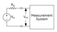
Figure 1. Voltage Signal Source and Measurement System Model
A voltage source can be grouped into one of two categories—grounded or ungrounded (floating). Similarly, a measurement system can be grouped into one of two categories—grounded or ground-referenced, and ungrounded (floating).
Grounded or Ground-Referenced Signal Source
A grounded source is one in which the voltage signal is referenced to the building system ground. The most common example of a grounded source is any common plug-in instrument that does not explicitly float its output signal. Figure 2 shows a grounded signal source.
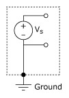
Figure 2. Grounded Signal Source
The grounds of two grounded signal sources will generally not be at the same potential. The difference in ground potential between two instruments connected to the same building power system is typically on the order of 10 mV to 200 mV; however, the difference can be higher if power distribution circuits are not properly connected.
Ungrounded or Nonreferenced (Floating) Signal Source
A floating source is a source in which the voltage signal is not referred to an absolute reference, such as earth or building ground. Some common examples of floating signal sources are batteries, battery powered signal sources, thermocouples, transformers, isolation amplifiers, and any instrument that explicitly floats its output signal. A nonreferenced or floating signal source is depicted in Figure 3.
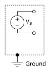
Figure 3. Floating or Nonreferenced Signal Source
Notice that neither terminal of the source is referred to the electrical outlet ground. Thus, each terminal is independent of earth.
Differential or Nonreferenced Measurement System
A differential, or nonreferenced, measurement system has neither of its inputs tied to a fixed reference such as earth or building ground. Hand-held, battery-powered instruments and data acquisition devices with instrumentation amplifiers are examples of differential or nonreferenced measurement systems. Figure 4 depicts an implementation of an 8-channel differential measurement system used in a typical device from NI. Analog multiplexers are used in the signal path to increase the number of measurement channels while still using a single instrumentation amplifier. For this device, the pin labeled AI GND, the analog input ground, is the measurement system ground.
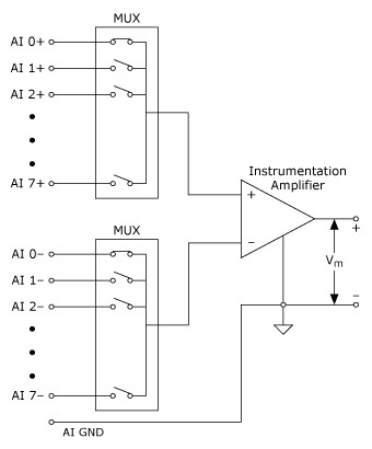
Figure 4. An 8-Channel Differential Measurement System
An ideal differential measurement system responds only to the potential difference between its two terminals—the (+) and (–) inputs. Any voltage measured with respect to the instrumentation amplifier ground that is present at both amplifier inputs is referred to as a common-mode voltage. Common-mode voltage is completely rejected (not measured) by an ideal differential measurement system. This capability is useful in rejection of noise, as unwanted noise is often introduced in the circuit making up the cabling system as common-mode voltage. Practical devices, however, have several limitations, described by parameters such as common-mode voltage range and common-mode rejection ratio (CMRR), which limit this ability to reject the common-mode voltage.
Common-mode voltage Vcm is defined as follows:
where V+ = Voltage at the noninverting terminal of the measurement system with respect to the measurement system ground, V– = Voltage at the inverting terminal of the measurement system with respect to the measurement system ground and CMRR in dB is defined as follows:
A simple circuit that illustrates the CMRR is shown in Figure 5. In this circuit, CMRR in dB is measured as 20 log Vcm/Vout where V+ = V– = Vcm.
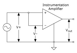
Figure 5. CMRR Measurement Circuit
The common-mode voltage range limits the allowable voltage swing on each input with respect to the measurement system ground. Violating this constraint results not only in measurement error but also in possible damage to components on the device. As the term implies, the CMRR measures the ability of a differential measurement system to reject the common-mode voltage signal. The CMRR is a function of frequency and typically reduces with frequency. The CMRR can be optimized by using a balanced circuit. This issue is discussed in more detail later in this application note. Most data acquisition devices will specify the CMRR up to 60 Hz, the power line frequency.
Grounded or Ground-Referenced Measurement System
A grounded or ground-referenced measurement system is similar to a grounded source in that the measurement is made with respect to ground. Figure 6 depicts an 8-channel grounded measurement system. This is also referred to as a single-ended measurement system.
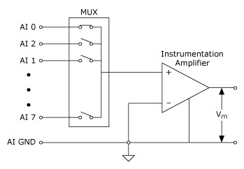
Figure 6. An 8-Channel Ground-Referenced Single-Ended (RSE) Measurement System
A variant of the single-ended measurement technique, known as nonreferenced single-ended (NRSE), is often found in data acquisition devices. A NRSE measurement system is depicted in Figure 7.
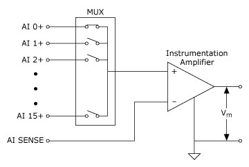
Figure 7. An 8-Channel NRSE Measurement System
In an NRSE measurement system, all measurements are still made with respect to a single-node Analog Input Sense (AI SENSE), but the potential at this node can vary with respect to the measurement system ground (AI GND). Figure 7 illustrates that a single-channel NRSE measurement system is the same as a single-channel differential measurement system.
Now that we have identified the different signal source type and measurement systems, we can discuss the proper measurement system for each type of signal source.
Measuring Grounded Signal Sources
A grounded signal source is best measured with a differential or nonreferenced measurement system. Figure 8 shows the pitfall of using a ground-referenced measurement system to measure a grounded signal source. In this case, the measured voltage, Vm, is the sum of the signal voltage, Vs, and the potential difference, DVg, that exists between the signal source ground and the measurement system ground. This potential difference is generally not a DC level; thus, the result is a noisy measurement system often showing power-line frequency (60 Hz) components in the readings. Ground-loop introduced noise may have both AC and DC components, thus introducing offset errors as well as noise in the measurements. The potential difference between the two grounds causes a current to flow in the interconnection. This current is called ground-loop current.
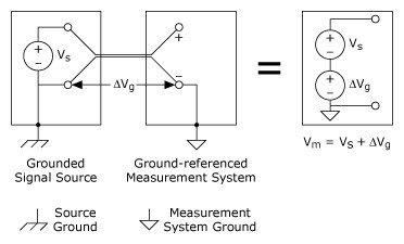
Figure 8. A Grounded Signal Source Measured with a Ground-Referenced System Introduces Ground Loop
A ground-referenced system can still be used if the signal voltage levels are high and the interconnection wiring between the source and the measurement device has a low impedance. In this case, the signal voltage measurement is degraded by ground loop, but the degradation may be tolerable. The polarity of a grounded signal source must be carefully observed before connecting it to a ground-referenced measurement system because the signal source can be shorted to ground, thus possibly damaging the signal source. Wiring considerations are discussed in more detail later in this application note.
A nonreferenced measurement is provided by both the differential (DIFF) and the NRSE input configurations on a typical data acquisition device. With either of these configurations, any potential difference between references of the source and the measuring device appears as common-mode voltage to the measurement system and is subtracted from the measured signal. This is illustrated in Figure 9.
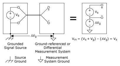
Figure 9. A Differential Measurement System Used to Measure a Grounded Signal Source
Measuring Floating (Nonreferenced) Sources
Floating signal sources can be measured with both differential and single-ended measurement systems. In the case of the differential measurement system, however, care should be taken to ensure that the common-mode voltage level of the signal with respect to the measurement system ground remains in the common-mode input range of the measurement device.
A variety of phenomena—for example, the instrumentation amplifier input bias currents—can move the voltage level of the floating source out of the valid range of the input stage of a data acquisition device. To anchor this voltage level to some reference, resistors are used as illustrated in Figure 10. These resistors, called bias resistors, provide a DC path from the instrumentation amplifier inputs to the instrumentation amplifier ground. These resistors should be of a large enough value to allow the source to float with respect to the measurement reference (AI GND in the previously described measurement system) and not load the signal source, but small enough to keep the voltage in the range of the input stage of the device. Typically, values between 10 kΩ and 100 kΩ work well with low-impedance sources such as thermocouples and signal conditioning module outputs. These bias resistors are connected between each lead and the measurement system ground.
Warning: Failure to use these resistors will result in erratic or saturated (positive full-scale or negative full-scale) readings.
If the input signal is DC-coupled, only one resistor connected from the (–) input to the measurement system ground is required to satisfy the bias current path requirement, but this leads to an unbalanced system if the source impedance of the signal source is relatively high. Balanced systems are desirable from a noise immunity point of view. Consequently, two resistors of equal value—one for signal high (+) input and the other for signal low (–) input to ground—should be used if the source impedance of the signal source is high. A single bias resistor is sufficient for low-impedance DC-coupled sources such as thermocouples. Balanced circuits are discussed further later in this application note.
If the input signal is AC-coupled, two bias resistors are required to satisfy the bias current path requirement of the instrumentation amplifier.
Resistors (10 kΩ < R < 100 kΩ) provide a return path to ground for instrumentation amplifier input bias currents, as shown in Figure 10. Only R2 is required for DC-coupled signal sources. For AC-coupled sources, R1 = R2.
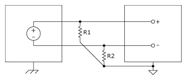
Figure 10. Floating Source and Differential Input Configuration
If the single-ended input mode is to be used, a RSE input system (Figure 11a) can be used for a floating signal source. No ground loop is created in this case. The NRSE input system (Figure 11b) can also be used and is preferable from a noise pickup point of view. Floating sources do require bias resistor(s) between the AI SENSE input and the measurement system ground (AI GND) in the NRSE input configuration.
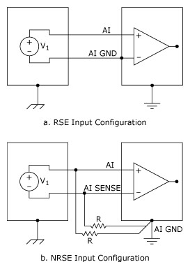
Figure 11. Floating Signal Source and Single-Ended Configurations
A graphic summary of the previous discussion is presented in Table 1.
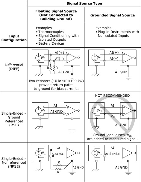
Table 1. Analog Input Connections
Note: Single-Ended-Ground Referenced (RSE) is not recommended when using a grounded signal source!
Warning: Bias resistors must be provided when measuring floating signal sources in DIFF and NRSE configurations. Failure to do so will result in erratic or saturated (positive full-scale or negative full-scale) readings.
In general, a differential measurement system is preferable because it rejects not only ground loop-induced errors, but also the noise picked up in the environment to a certain degree. The single-ended configurations, on the other hand, provide twice as many measurement channels but are justified only if the magnitude of the induced errors is smaller than the required accuracy of the data. Single-ended input connections can be used when all input signals meet the following criteria.
- Input signals are high level (greater than 1 V)
- Signal cabling is short and travels through a noise-free environment or is properly shielded
- All input signals can share a common reference signal at the source
Differential connections should be used when any of the above criteria are violated.
Minimizing Noise Coupling in the Interconnects
Even when a measurement setup avoids ground loops or analog input stage saturation by following the above guidelines, the measured signal will almost inevitably include some amount of noise or unwanted signal "picked up" from the environment. This is especially true for low-level analog signals that are amplified using the onboard amplifier that is available in many data acquisition devices. To make matters worse, PC data acquisition boards generally have some digital input/output signals on the I/O connector. Consequently, any activity on these digital signals provided by or to the data acquisition board that travels across some length in close proximity to the low-level analog signals in the interconnecting cable itself can be a source of noise in the amplified signal. In order to minimize noise coupling from this and other extraneous sources, a proper cabling and shielding scheme may be necessary.
Before proceeding with a discussion of proper cabling and shielding, an understanding of the nature of the interference noise-coupling problem is required. There is no single solution to the noise-coupling problem. Moreover, an inappropriate solution might make the problem worse.
An interference or noise-coupling problem is shown in Figure 12.
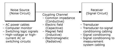
Figure 12. Noise-Coupling Problem Block Diagram
As shown in Figure 12, there are four principal noise "pick up" or coupling mechanisms—conductive, capacitive, inductive, and radiative. Conductive coupling results from sharing currents from different circuits in a common impedance. Capacitive coupling results from time-varying electric fields in the vicinity of the signal path. Inductive or magnetically coupled noise results from time-varying magnetic fields in the area enclosed by the signal circuit. If the electromagnetic field source is far from the signal circuit, the electric and magnetic field coupling are considered combined electromagnetic or radiative coupling.
Conductively Coupled Noise
Conductively coupled noise exists because wiring conductors have finite impedance. The effect of these wiring impedances must be taken into account in designing a wiring scheme. Conductive coupling can be eliminated or minimized by breaking ground loops (if any) and providing separated ground returns for both low-level and high-level, high-power signals. A series ground-connection scheme resulting in conductive coupling is illustrated in Figure 13a.
If the resistance of the common return lead from A to B is 0.1 Ω, the measured voltage from the temperature sensor would vary by 0.1 Ω * 1 A = 100 mV, depending on whether the switch is closed or open. This translates to 10° of error in the measurement of temperature. The circuit of Figure 13b provides separate ground returns; thus, the measured temperature sensor output does not vary as the current in the heavy load circuit is turned on and off.
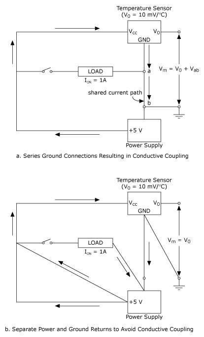
Figure 13. Conductively Coupled Noise
Capacitive and Inductive Coupling
The analytical tool required for describing the interaction of electric and magnetic fields of the noise and signal circuits is the mathematically nontrivial Maxwell’s equation. For an intuitive and qualitative understanding of these coupling channels, however, lumped circuit equivalents can be used. Figures 14 and 15 show the lumped circuit equivalent of electric and magnetic field coupling.
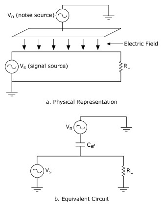
Figure 14. Capacitive Coupling between the Noise Source and Signal Circuit, Modeled by the Capacitor Cef in the Equivalent Circuit
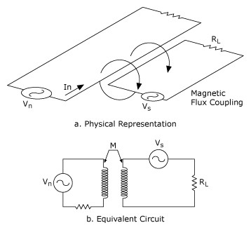
Figure 15. Inductive Coupling between the Noise Source and Signal Circuit, Modeled by the Mutual Inductance M in the Equivalent Circuit
Introduction of lumped circuit equivalent models in the noise equivalent circuit handles a violation of the two underlying assumptions of electrical circuit analysis; that is, all electric fields are confined to the interior of capacitors, and all magnetic fields are confined to the interior of inductors.
Capacitive Coupling
The utility of the lumped circuit equivalent of coupling channels can be seen now. An electric field coupling is modeled as a capacitance between the two circuits. The equivalent capacitance Cef is directly proportional to the area of overlap and inversely proportional to the distance between the two circuits. Thus, increasing the separation or minimizing the overlap will minimize Cef and hence the capacitive coupling from the noise circuit to the signal circuit. Other characteristics of capacitive coupling can be derived from the model as well. For example, the level of capacitive coupling is directly proportional to the frequency and amplitude of the noise source and to the impedance of the receiver circuit. Thus, capacitive coupling can be reduced by reducing noise source voltage or frequency or reducing the signal circuit impedance. The equivalent capacitance Cef can also be reduced by employing capacitive shielding. Capacitive shielding works by bypassing or providing another path for the induced current so it is not carried in the signal circuit. Proper capacitive shielding requires attention to both the shield location and the shield connection. The shield must be placed between the capacitively coupled conductors and connected to ground only at the source end. Significant ground currents will be carried in the shield if it is grounded at both ends. For example, a potential difference of 1 V between grounds can force 2 A of ground current in the shield if it has a resistance of 0.5 Ω. Potential differences on the order of 1 V can exist between grounds. The effect of this potentially large ground current will be explored further in the discussion of inductively coupled noise. As a general rule, conductive metal or conductive material in the vicinity of the signal path should not be left electrically floating either, because capacitively coupled noise may be increased.
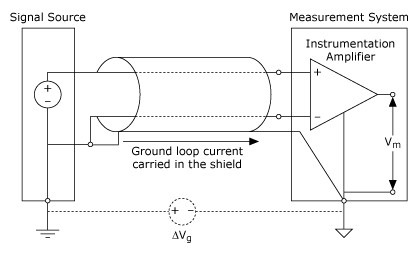
Figure 16. Improper Shield Termination—Ground Currents Are Carried in the Shield
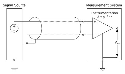
Figure 17. Proper Shield Termination—No Ground or Signal Current Flows through the Shield
Inductive Coupling
As described earlier, inductive coupling results from time-varying magnetic fields in the area enclosed by the signal circuit loop. These magnetic fields are generated by currents in nearby noise circuits. The induced voltage Vn in the signal circuit is given by the formula:
where f is the frequency of the sinusoidally varying flux density, B is the rms value of the flux density, A is the area of the signal circuit loop, and Æ is the angle between the flux density B and the area A.
The lumped circuit equivalent model of inductive coupling is the mutual inductance M as shown in Figure 15(b). In terms of the mutual inductance M, Vn is given by the formula:
where In is the rms value of the sinusoidal current in the noise circuit, and f is its frequency.
Because M is directly proportional to the area of the receiver circuit loop and inversely proportional to the distance between the noise source circuit and the signal circuit, increasing the separation or minimizing the signal loop area will minimize the inductive coupling between the two circuits. Reducing the current In in the noise circuit or reducing its frequency can also reduce the inductive coupling. The flux density B from the noise circuit can also be reduced by twisting the noise source wires. Finally, magnetic shielding can be applied either to noise source or signal circuit to minimize the coupling.
Shielding against low-frequency magnetic fields is not as easy as shielding against electric fields. The effectiveness of magnetic shielding depends on the type of material—its permeability, its thickness, and the frequencies involved. Due to its high relative permeability, steel is much more effective than aluminum and copper as a shield for low-frequency (roughly below 100 kHz) magnetic fields. At higher frequencies, however, aluminum and copper can be used as well. Absorption loss of copper and steel for two thicknesses is shown in Figure 18. The magnetic shielding properties of these metals are quite ineffective at low frequencies such as those of the power line (50 to 60 Hz), which are the principal low-frequency, magnetically-coupled noise sources in most environments. Better magnetic shields such as Mumetal can be found for low-frequency magnetic shielding, but Mumetal is very fragile and can have severe degradation of its permeability, and hence, degradation of its effectiveness as a magnetic shield by mechanical shocks.
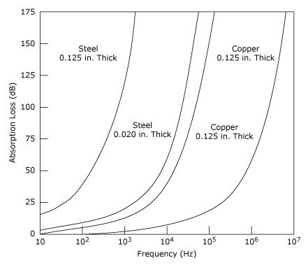
Figure 18. Absorption Loss as a Function of Frequency (from Reference 1)
Because of the lack of control over the noise circuit parameters and the relative difficulty of achieving magnetic shielding, reducing the signal circuit loop area is an effective way to minimize inductive coupling. Twisted-pair wiring is beneficial because it reduces both the loop area in the signal circuit and cancels induced errors.
Formula (2) determines the effect of carrying ground-loop currents in the shield for the circuit in Figure 16. For In = 2 A; f = 60 Hz; and M = 1 µH/ft for a 10-ft cable results in the following:
This noise level translates into 3.1 LSB for a 10 V range, 12-bit data acquisition system. The effectiveness of the data acquisition system is thus reduced roughly to that of a 10-bit acquisition system.
When using an E Series device with a shielded cable in differential mode, the signal circuit loop area is minimized because each pair of signal leads is configured as a twisted pair. This is not true for the single-ended mode with the same device and cable because loop areas of different sizes may be formed with different channels.
Current signal sources are more immune to this type of noise than voltage signal sources because the magnetically induced voltage appears in series with the source, as shown in Figure 19. V21 and V22 are inductively coupled noise sources, and Vc is a capacitively coupled noise source.
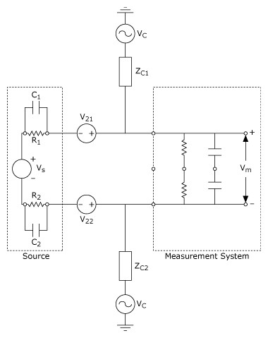
Figure 19. Circuit Model of Inductive and Capacitive Noise Voltage Coupling
(H. W. Ott, Noise Reduction Techniques in Electronic Systems, Wiley, 1976.)
The level of both inductive and capacitive coupling depends on the noise amplitude and the proximity of the noise source and the signal circuit. Thus, increasing separation from interfering circuits and reducing the noise source amplitude are beneficial. Conductive coupling results from direct contact; thus, increasing the physical separation from the noise circuit is not useful.
Radiative Coupling
Radiative coupling from radiation sources such as radio and TV broadcast stations and communication channels would not normally be considered interference sources for the low-frequency (less than 100 kHz) bandwidth measurement systems. But high-frequency noise can be rectified and introduced into low-frequency circuits through a process called audio rectification. This process results from the nonlinear junctions in ICs acting as rectifiers. Simple passive R-C lowpass filters at the receiver end of long cabling can reduce audio rectification.
The ubiquitous computer terminal is a source of electric and magnetic field interference in nearby sensitive circuits. This is illustrated in Figure 20, which shows the graphs of data obtained with a data acquisition device using a gain of 500 with the onboard programmable gain amplifier. The input signal is a short circuit at the termination block. A 0.5 m unshielded interconnecting cable was used between the terminal block and the device I/O connector. For differential signal connection, the channel high and channel low inputs were tied together and to the analog system ground. For the single-ended connection, the channel input was tied to the analog system ground.
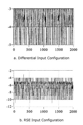
Figure 20. Noise Immunity of Differential Input Configuration Compared with that of RSE Configuration (DAQ board gain: 500; Cable: 0.5 m Unshielded; Noise Source: Computer Monitor)
Miscellaneous Noise Sources
Whenever motion of the interconnect cable is involved, such as in a vibrational environment, attention must be paid to the triboelectric effect, as well as to induced voltage due to the changing magnetic flux in the signal circuit loop. The triboelectric effect is caused by the charge generated on the dielectric within the cable if it does not maintain contact with the cable conductors.
Changing magnetic flux can result from a change in the signal circuit loop area caused by motion of one or both of the conductors—just another manifestation of inductive coupling. The solution is to avoid dangling wires and to clamp the cabling.
In measurement circuits dealing with very low-level circuits, attention must be paid to yet another source of measurement error—the inadvertent thermocouples formed across the junctions of dissimilar metals. Errors due to thermocouple effects do not constitute interference type errors but are worth mentioning because they can be the cause of mysterious offsets between channels in low-level signal measurements.
Balanced Systems
In describing the differential measurement system, it was mentioned that the CMRR is optimized in a balanced circuit. A balanced circuit is one that meets the following three criteria:
- The source is balanced—both terminals of the source (signal high and signal common) have equal impedance to ground.
- The cable is balanced—both conductors have equal impedance to ground.
- The receiver is balanced—both terminals of the measurement end have equal impedance to ground.
Capacitive pickup is minimized in a balanced circuit because the noise voltage induced is the same on both conductors due to their equal impedances to ground and to the noise source.
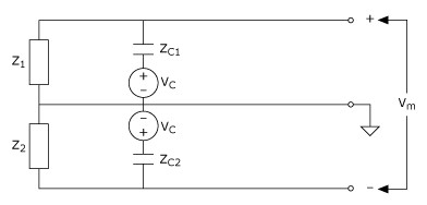
Figure 21. Capacitive Noise Coupling Circuit Model
(H.W. Ott, Noise Reduction Techniques in Electronic Systems, Wiley, 1976.)
If the circuit model of Figure 21 represented a balanced system, the following conditions would apply:
Simple circuit analysis shows that for the balanced case V+ = V–, the capacitively coupled voltage Vc appears as a common-mode signal. For the unbalanced case, that is, either Z1<> Z2 or Zc1<>Zc2, the capacitively coupled voltage Vc appears as a differential voltage, that is, V+<>V–, which cannot be rejected by an instrumentation amplifier. The higher the imbalance in the system or mismatch of impedances to ground and the capacitive coupling noise source, the higher the differential component of the capacitively coupled noise will be.
A differential connection presents a balanced receiver on the data acquisition device side of the cabling, but the circuit is not balanced if either the source or the cabling is not balanced. This is illustrated in Figure 22. The data acquisition device is configured for differential input mode at a gain of 500. The source impedance Rs was the same (1 kΩ) in both the setups. The bias resistors used in the circuit of Figure 22b are both 100 kΩ. The common-mode rejection is better for the circuit in Figure 22b than for Figure 22a. Figure 22c and 22d are time-domain plots of the data obtained from configurations 22a and 22b respectively. Notice the absence of noise-frequency components with the balanced source configuration. The noise source in this setup was the computer monitor. The balanced setup also loads the signal source with
This loading effect should not be ignored. The unbalanced setup does not load the signal source.
In a setup such as the one in Figure 22a, the imbalance in the system (mismatch in impedance to ground from the signal high and low conductors) is proportional to the source impedance Rs. For the limiting case Rs = 0 Ω, the setup in Figure 22a is also balanced, and thus less sensitive to noise.
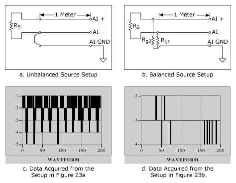
Figure 22. Source Setup and the Acquired Data
Twisted pairs or shielded, twisted pairs are examples of balanced cables. Coaxial cable, on the other hand, is not balanced because the two conductors have different capacitance to ground.
Source Impedance Characteristics
Because the source impedance is important in determining capacitive noise immunity of the cabling from the source to the data acquisition system, the impedance characteristics of some of the most common transducers are listed in Table 2.
Transducer
| Impedance Characteristic
|
Thermocouples
| Low (<20 ohm)
|
Thermistors
| High (>1 kohm)
|
Resistance Temperature Detector
| Low (<1 kohm)
|
Solid-State Pressure Transducer
| High (>1 kohm)
|
Strain Gauges
| Low (<1 kohm)
|
Glass pH Electrode
| Very High (1 Gohm)
|
Potentiometer (Linear Displacement)
| High (500 ohm to 100 kohm)
|
High-impedance, low-level sensor outputs should be processed by a signal conditioning stage located near the sensor.
Solving Noise Problems in Measurement Setups
Solving noise problems in a measurement setup must first begin with locating the cause of the interference problem. Noise problems could be anything from the transducer to the data acquisition device itself. A process of trial and elimination could be used to identify the culprit.
The data acquisition device itself must first be verified by presenting it with a low-impedance source with no cabling and observing the measurement noise level. This can be done easily by short circuiting the high and low signals to the analog input ground with as short a wire as possible, preferably at the I/O connector of the data acquisition device. The noise levels observed in this trial will give you an idea of the best case that is possible with the given data acquisition device. If the noise levels measured are not reduced from those observed in the full setup (data acquisition device plus cabling plus signal sources), then the measurement system itself is responsible for the observed noise in the measurements. If the observed noise in the data acquisition device is not meeting its specifications, one of the other devices in the computer system may be responsible.
Try removing other boards from the system to see if the observed noise levels are reduced. Changing board location, that is, the slot into which the data acquisition board is plugged, is another alternative.
The placement of computer monitors could be suspect. For low-level signal measurements, it is best to keep the monitor as far from the signal cabling and the computer as possible. Setting the monitor on top of the computer is not desirable when acquiring or generating low-level signals.
Cabling from the signal conditioning and the environment under which the cabling is run to the acquisition device can be checked next if the acquisition device has been dismissed as the culprit. The signal conditioning unit or the signal source should be replaced by a low-impedance source, and the noise levels in the digitized data observed. The low-impedance source can be a direct short of the high and low signals to the analog input ground. This time, however, the short is located at the far end of the cable. If the observed noise levels are roughly the same as those with the actual signal source instead of the short in place, the cabling and/or the environment in which the cabling is run is the culprit. Cabling reorientation and increasing distance from the noise sources are possible solutions. If the noise source is not known, spectral analysis of the noise can identify the interference frequencies, which in turn can help locate the noise source. If the observed noise levels are smaller than those with the actual signal source in place, however, a resistor approximately equal to the output resistance of the source should be tried next in place of the short at the far end of the cable. This setup will show whether capacitive coupling in the cable due to high source impedance is the problem. If the observed noise levels from this last setup are smaller than those with the actual signal in place, cabling and the environment can be dismissed as the problem. In this case, the culprit is either the signal source itself or improper configuration of the data acquisition device for the source type.
Signal Processing Techniques for Noise Reduction
Although signal processing techniques are not a substitute for proper system interconnection, they can be employed for noise reduction, as well. All noise-reducing signal processing techniques rely on trading off signal bandwidth to improve the signal-to-noise ratio. In broad terms, these can be categorized as preacquisition or postacquisition measures. Examples of preacquisition techniques are various types of filtering (lowpass, highpass, or bandpass) to reduce the out-of-band noise in the signal. The measurement bandwidth need not exceed the dynamics or the frequency range of the transducer. Postacquisition techniques can be described as digital filtering. The simplest postacquisition filtering technique is averaging. This results in comb filtering of the acquired data and is especially useful for rejecting specific interference frequencies such as 50 to 60 Hz. Remember that inductive coupling from low-frequency sources such as 50 Hz to 60 Hz power lines is harder to shield against. For optimal interference rejection by averaging, the time interval of the acquired data used for averaging, Tacq, must be an integral multiple of Trej = 1/ Frej, where Frej is the frequency being optimally rejected.
where Ncycles is the number of cycles of interfering frequency being averaged. Because Tacq = Ns ´ Ts where Ns is the number of samples used for averaging and Ts is the sampling interval, equation (1) can be written as follows:
or
Equation (4) determines the combination of the number of samples and the sampling interval to reject a specific interfering frequency by averaging. For example, for 60 Hz rejection using Ncycles = 3 and Ns = 40, we can calculate the optimal sampling rate as follows:
Thus, averaging 40 samples acquired at a sampling interval of 1.25 ms (or 800 samples/s) will reject 60 Hz noise from the acquired data. Similarly, averaging 80 samples acquired at 800 samples/s (10 readings/s) will reject both 50 and 60 Hz frequencies. When using a lowpass digital filtering technique, such as averaging, you cannot assume that the resultant data has no DC errors such as offsets caused by ground loops. In other words, if a noise problem in a measurement system is resolved by averaging, the system may still have DC offset errors. The system must be verified if absolute accuracy is critical to the measurements.
References
- Ott, Henry W., Noise Reduction Techniques in Electronic Systems. New York: John Wiley & Sons, 1976.
- Barnes, John R., Electronic System Design: Interference and Noise Control Techniques, New Jersey: Prentice-Hall, Inc., 1987.