LabVIEW FPGA Design for Code Modules (IP Cores)
Overview
Contents
- IPNet FPGA Guidelines at a Glance
- FPGA IP – Reusable Code Modules
- Scalable IP
- Internal Data Storage
- Timing Independence
- Project Independence
- I/O Module Independence
- Performance
- Documentation, Testing, and Examples
- Summary
IPNet FPGA Guidelines at a Glance
Scalable IP
| Scalable IP should allow for multiple blocks to be used together to access increasing amounts of I/O or required memory | 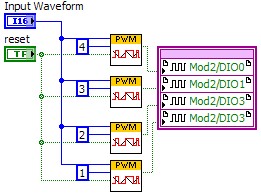 |
Internal Data Storage
| Feedback nodes access data points from previous iterations and pipelining |  |
| VI scoped dual port memory and FIFOs allow for FPGA memory access without the use of the LabVIEW Project
|  |
Timing Independence
| Avoid Using loop structures. Use loops outside of IP Block
|  |
| Do not using timing functions to delay the IP Block
|  |
Project Independence
| IP should not require the configuration in the project
|  |
| Avoid using the FPGA wizard
|  |
I/O Module Independence
| Access I/O Nodes from the calling VI | 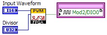 |
| Or use the FPGA I/O constant to address a module and channel.
|  |
Performance
| Pipelining is the use of feedback nodes or shift registers in order to allow items that would normally execute serially to execute in parallel | 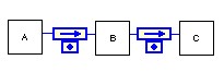 |
| The Single Cycle Timed Loop is a LabVIEW Timed Loop Structure used in LabVIEW FPGA. A SCTL allows for all the code within the loop to execute in one tick of the FPGA clock. | 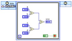 |
FPGA IP – Reusable Code Modules
Any software development effort includes the development of functions, subroutines, objects, code modules, or other basic building blocks of the larger architecture. As you design an application, you identify and implement individual functions and operations. Later on you can combine and integrate these building blocks to form the larger application. Through the process of developing different applications over time, a group or community of developers creates libraries of code modules representing common operations and reuses them to build future applications more quickly. The purpose of developing such libraries of code is to reduce the overall development effort by building and testing a function once and reusing it many times. Besides promoting the reuse of existing code, modular design also increases code testability and maintainability, so developers and designers can focus on application-specific features and code segments.
The LabVIEW language has a set of guidelines used by programmers worldwide to develop subVIs that can be easily understood, applied in different applications, and maintained by different developers. When using NI LabVIEW FPGA to develop applications for FPGA deployment, you need to follow some additional guidelines for building code modules (subVIs) that take advantage of FPGA-specific behavior. This helps you apply the subVIs efficiently in a wide range of FPGA-based applications.
On the FPGA platform, reusable code modules are commonly called IP (intellectual property) cores; the name evolved over time from traditional chip design. In LabVIEW FPGA, these IP cores consist of subVIs, commonly used in LabVIEW programming and LabVIEW toolkits. With subVIs in LabVIEW FPGA, you can implement different functions and operations once, optimize their implementation for the FPGA platform, and apply them in different applications. To further promote and improve the reuse of LabVIEW FPGA IP, code modules should incorporate some components in addition to the subVI source code. These include documentation, test code, and basic IP use examples.
In LabVIEW FPGA applications, IP code modules might perform a variety of operations including encoding and decoding data using a communication protocol (SPI, I2C, etc), digital signal processing (filtering, FFT, etc), implementation of control algorithms (PID, etc), sensor encoding/decoding (PWM, quadrature signal, etc), triggering, and benchmarking.
Scalable IP
IP blocks conditioning a signal for output or input or accessing VI scoped memory should be written such they can access as little or as much I/O necessary for any application. This reduces the FPGA footprint for each piece of IP by not including additional code for additional inputs, outputs, or memory spaces.
Some applications may use multiple copies of an IP code module, and the code module should support such operations seamlessly. If the code module subVI uses any local variables to store state information, then set the subVI to be reentrant. This creates multiple instances of the subVI, each with its own memory space for state information, on the FPGA during the compile process.
IO Scalabilty
If additional IO is required the user should be able to drop down an additional IP block for each IO point. In order to keep the block diagram organized multiple pieces of IP can be wrapped in a single subVI. If an IP Block contains application specific code along with more generic code, consider making each of these a distinct piece of IP. This improves the modularity and scalability of each piece of IP.
Memory Scalability
Like IO scalability any single piece of IP should only be able to access a single space in memory of FIFO. The FIFOs and memory spaces should not be included within the IP itself, but instead is accessed from the calling VI.
Some applications may use multiple copies of an IP code module, and the code module should support such operations seamlessly. If the code module subVI uses any local variables to store state information, then set the subVI to be reentrant. This creates multiple instances of the subVI, each with its own memory space for state information, on the FPGA during the compile process.
Internal Data Storage
Depending on the functionality of your IP, it may require some type of data storage element internal to your subVI. There are two main mechanisms for data storage inside IP: feedback nodes and VI-scoped memory. Feedback nodes, which store one data point between iterations, are effective at maintaining the most recent value as well as implementing pipelines to improve algorithm throughput. VI-scoped memory allows for dedicated blocks of dual port memory or VI-scoped first-in-first-out memory buffers (FIFOs). It is important to avoid FIFOs created in the LabVIEW Project whenever possible. Using LabVIEW Project FIFOs makes IP less modular because it depends on LabVIEW Project configurations. Using global memory is necessary only when the IP requires custom buffered inputs and outputs.
Feedback Node
As of the LabVIEW FPGA Module 8.5, you can place the feedback node anywhere in the block diagram. The feedback node performs the same function as a shift register – maintaining the value of the last iteration.
outputi = inputi-1
Use feedback nodes to store state information between iterations of an iterative algorithm. Take a simple counter for example. Figure 1 illustrates using the feedback node to access the previous count and increment on an edge.
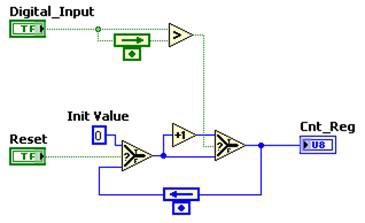
Figure 1. Using the Feedback Node to Access the Previous Count and Increment on an Edge in a Simple Counter
Before the improved feedback node in the LabVIEW FPGA Module 8.5, there were other options for storing state information in a subVI. The most common was the LabVIEW functional global, which encapsulates subVI code in a single-iteration while loop with an un-initialized shift register to store state data. Because this technique was not compatible with a single-cycle timed loop, it was not recommended for LabVIEW FPGA implementation.
Using front panel indicators and controls to store data was also an option before the release of the LabVIEW FPGA Module 8.5. You can read and write to these front panel objects with a local variable, and the front panel object acts like the storage register. Unlike LabVIEW for Windows, local variables are not discouraged in LabVIEW FPGA because there is no extra overhead in reading and writing this storage element. Furthermore, as long as the control lies in a subVI, there is no extra logic for host communication like there is in the top-level VI. This method is compatible within a single-cycle timed loop because it does not require a loop to implement state storage.
Note: In LabVIEW FPGA, the feedback node becomes a hardware flip-flop. When placed between functions, the feedback node acts as a pipeline stage.
The LabVIEW FPGA Module 8.5 feedback node is an elegant way to store a single data value across iterations of an IP block. This method is recommended over the functional global and the local variable techniques. Additionally, the feedback node is the recommended way to store data passing between pipeline stages.
Block Memory
In addition to feedback nodes, a storage resource LabVIEW FPGA IP could potentially use is block (user) memory, or user-accessible memory blocks on the FPGA itself.
FPGA Part | NI Products | Block RAM |
| 1M gate Virtex-II | R Series Multifunction RIO – NI 7811R, CompactRIO backplanes – cRIO-9101, cRIO-9102 | 720 Kb |
| 3M gate Virtex-II | R Series Multifunction RIO – CompactRIO backplanes – cRIO-9103, cRIO-9104 | 1728 Kb |
| 1M gate Spartan-3 | CompactRIO integrated system – Single-Board RIO – sbRIO-9601, sbRIO-9611, sb-RIO 9631, sbRIO-9641 | 432 Kb |
| 2M gate Spartan-3 | CompactRIO integrated system – Single-Board RIO – sbRIO-9602, sbRIO-9612, sbRIO-9632, sbRIO-9642 EtherCAT – NI 9144 Ethernet – NI 9148 | 720 Kb |
| Virtex-5 LX30 | R Series Multifunction RIO – NI 7851R, NI 7841R CompactRIO backplanes – cRIO-9111, cRIO-9112 FlexRIO – PXI-7951R | 1152 Kb |
| Virtex-5 LX50 | R Series Multifunction RIO – NI 7852R, NI 7842R CompactRIO backplanes – cRIO-9113, cRIO-9114 MXI-Express – NI 9154 | 1728 Kb |
| Virtex-5 LX85 | R Series Multifunction RIO – NI 7853R CompactRIO backplanes – cRIO-9116 FlexRIO – PXI-7953R MXI-Express – NI 9155, NI 9157 | 3456 Kb |
| Virtex-5 LX110 | R Series Multifunction RIO – NI 7854R CompactRIO backplanes – cRIO-9118 FlexRIO – PXI-7954R MXI-Express – NI 9159 | 4608 Kb |
| Virtex-5 SX50T | FlexRIO – PXIe-7961R, PXIe-7962R
| 4752 Kb |
| Virtex-5 SX95T | FlexRIO – PXIe-7965R, PXIe-7966R
| 8784 Kb |
| Spartan 6 LX25 | CompactRIO integrated system – cRIO-9075 Single-Board RIO – sbRIO-9605, sbRIO-9623, sbRIO-9633 | 936 Kb |
| Spartan-6 LX45 | CompactRIO Integrated System – cRIO-9076 Single-Board RIO – sbRIO-9606, sbRIO-9626, sbRIO-9636 Ethernet – NI 9146 | 2088 Kb |
| Spartan-6 LX75 | CompactRIO Integrated System – cRIO-9081
| 3096 Kb |
| Spartan-6 LX150 | CompactRIO Integrated System – cRIO-9082
| 4824 Kb |
| Artix-7 Zync 7020 | CompactRIO Integrated System – cRIO-9068
| 560 Kb |
| Kintex-7 70T | R Series Multifunction RIO – NI USB-7855R, NI USB-7855R OEM
| 4860 Kb |
| Kintex-7 160T | R Series Multifunction RIO – NI USB-7856R, NI USB-7856R OEM
| 11700 Kb |
| Kintex-7 410T | FlexRIO – PXIe-7975R
| 28620 Kb |
Table 1. Another LabVIEW FPGA storage resource is user-accessible memory blocks on the FPGA itself.
Use this type of storage when your IP requires many data points or necessitates an internal FIFO. With LabVIEW FPGA, you can access the block memory on the FPGA in a number of different ways including memory read/write, FIFOs, and lookup tables. For IP, it is important to create a unique space of memory usable only by the function itself. You can implement this with VI-scoped memory and FIFOs. Using global memory and FIFOs for IP is not recommended because your IP would have an unnecessary dependence on LabVIEW Project configurations.
However, LabVIEW FPGA Module 8.0 Memory Read and Memory Write functions use one common address space of 16 KB for all instances of these functions incorporated in any VI that is part of the current FPGA personality. Do not use these functions because they may cause a conflict with the memory you used elsewhere in the application. If random memory access is required in an IP code module developed in LabVIEW FPGA 8.0 (or earlier), you should use a memory block created using the LabVIEW Memory Extension Utility.
In LabVIEW 8.2 and later, each Memory Read and Memory Write function references a specific memory block (address space) that is typically created as a resource in the LabVIEW Project. Because these memory blocks are defined in the project, they are not automatically transferred to a new project if you load an IP code module VI in a new application. For this purpose, you can define a memory block in a VI as a VI-scoped memory configuration instead of a LabVIEW Project memory block. You can create and use a VI-scoped memory block in your IP, and it is automatically created in any new application where you use the IP
Similarly, the FPGA IP FIFO functions, which use block memory to buffer data, are based on a FIFO resource you create in the LabVIEW Project. If you decide to use a FIFO inside an IP code module in LabVIEW FPGA 8.0, the IP user is required to manually create the associated FIFO resource in the application project. To eliminate this additional requirement, avoid using FIFOs with any IP code module in LabVIEW FPGA 8.0.
In LabVIEW 8.2 and later, you have the option to develop a VI-scoped FIFO configuration to create a VI-specific FIFO memory block. Follow the same process you used for the VI-scoped memory block.
Regardless of how memory is used by the IP code module or the rest of the application, it is allocated from the common block memory available on the FPGA, which varies in size depending on the specific FPGA you use in the target. Therefore, it is important for a user of your IP code module to know how much memory, if any, is used by your IP. This information should be included in the documentation and context sensitive help. Developers using IP modules must keep track of the amount of block memory used by different parts of their applications to prevent a possible memory over allocation during compilation.
Timing Independence
To be able to freely use IP modules in a LabVIEW FPGA application, the code modules must not significantly affect the timing of the main application. For example, when processing two digital input signals from a quadrature encoder, the code module decoding the position information should not significantly delay the calling application. This means that the IP code module subVI should perform its action in a fast and efficient manner. In most cases, this means that there should not be any loop structures within the subVI. Also the subVI should not use any timing functions that delay the code. If you require timing or looping as part of the main application, you should implement it in the calling VI.
One exception to this guideline of making an IP code module’s timing independent of its caller is if the purpose of the IP code module is to provide timing functionality to the calling application. An example of this type of IP code module is a data acquisition scan clock utility. Figure 4 shows a simple IP code module that implements a scan clock with the added functionality of verifying that the calling application is able to meet the specified timing. You can quickly use this enhanced scan clock in many different applications. In this case, you should document the operation and timing dependence of the IP code module well so that users of the IP understand how the timing behavior of their applications will be affected.
Figure 4. Diagram of a IP Code Module That Implements a Scan Clock and Verifies That the Calling Application Meets Specified Timing
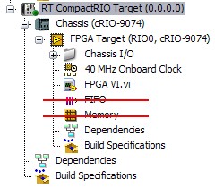
Project Independence
High quality IP should be highly independent and self contained. When creating IP you should be sure the IP has no dependency on the LabVIEW Project it was created in. This places some restrictions on the code within the IP code modules. However, these limitations are similar to the guidelines presented in the section on Internal Data Storage.
- Avoid using Project scoped FIFOs and Memory Blocks
- Avoid using the FPGA wizard
As of LabVIEW 8.2 and later we have the ability to use VI scoped FIFOs and Memory blocks. These provide the same functionality as project scoped FIFOs and Memory.
You should avoid using the LabVIEW FGPA Wizard because the wizard will always generate code that is dependent on the LabVIEW project.
I/O Module Independence
So that LabVIEW FPGA IP is easy to apply in different applications, make sure it is independent of any I/O channels or other hardware resources such as FPGA block memory. Depending on the individual application, users can incorporate different reconfigurable I/O devices or other FPGA targets in the final application. Therefore, you should not program the IP code module to a specific type of I/O resource. The programmer or developer integrating the IP module in the final application chooses which specific I/O resources to use. Data and values pertaining to I/O resources should be passed into the IP module as a parameter or be returned from the IP module.
For example, in the case of a pulse-width modulation (PWM) output IP module, the application developer chooses which digital output line to use for the PWM output signal. In this case, the PWM IP module should generate and output the current state of the signal. The developer assigns the value to the I/O resource in the higher-level VI. The I/O resource is not embedded in the diagram of the IP code module.
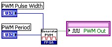
Figure 2. Diagram of an Application VI Calling the PWM Output IP Code Module (SubVI)
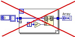
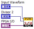
The same guideline applies to any input signals. For example, if you are using an analog filter IP subVI created in the NI Digital Filter Design Toolkit, you should acquire the analog value outside of the filter subVI and pass it into the IP code module.
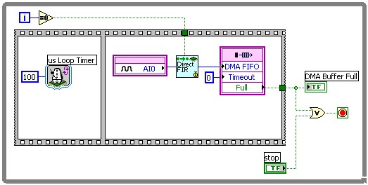
Figure 3. For analog filter IP subVIs created in the NI Digital Filter Toolkit, acquire the analog value outside of the filter subVI and pass it into the IP code module.
Developing IP code modules independently of I/O resources makes them easier and more flexible to use, and you can integrate them many times in an application without the need to customize each instance of the IP code module.
Performance
Efficient FPGA algorithms can be further improved by implementing one of the following methods or a combination of both.
Pipelining allows for code that would normally execute serially over several clock cycles to execute in parallel in fewer clock cycles. This is done by breaking up the subdiagram into discrete steps each of which become an independent stage of the pipeline. In each call of the code each stage of the pipeline processes the data point processed by the previous stage in the last call of the subdiagram. Pipelining can be implemented using shift registers or feedback nodes. For more information on Pipelining refer to Pipelining to Optimize FPGA VIs (FPGA Module) in the LabVIEW Help.
A Single Cycle Timed Loop (SCTL) is a special use of the Timed Loop Structure. The SCTL executes all code within the structure in one tick of the 40MHz FPGA clock or another derived clock. If a SCTL contains too much code to execute within one clock tick or contains and unsupported function or structure the user will receive a compile error. For a detailed list of functions that cannot be used in a SCTL please refer to Timed Loop Topic of LabVIEW Help for a full list of unsupported functions and structures.
Optimize performance for non-iterating code for size and speed by using a SCTL with a True Boolean constant wired to the conditional terminal
Documentation, Testing, and Examples
While developing an IP code module, you should create documentation, testing, and building examples as a required part of the development process. Other developers not familiar with the code module need information on how to the use the IP properly to implement it in their own applications.
As part of the implementation, you should include LabVIEW context help with each subVI that other developers will use. The context help is displayed in LabVIEW when the Help window is open and the mouse cursor hovers over the subVI. This documentation should include a basic description of the VI operation/function, as well as a basic description of each input and output parameter. You should also note any other programming limitations or restrictions pertaining to the subVI such as use in a single-cycle timed loop or block memory usage. Include more detailed descriptions of the VI and its parameters in a separate user or reference manual document.
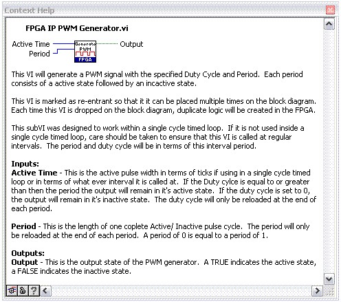
Figure 5. Include LabVIEW context help with each subVI that other developers will use.
Once you have completed the basic implementation of the IP code module, testing and building examples are the next logical development steps. Testing ensures that the IP code module performs as desired across all intended ranges. Test the IP code module with a range of different input values and in different programming scenarios beyond those originally considered. Also test multiple instances of the IP and multiple uses within different programming structures.
The final IP code module should include some basic and possibly more advanced examples that illustrate how the code module is to be used in an application. Often these examples are the starting point for an application centered on a particular IP.
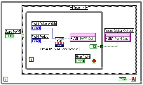
Figure 6. Include examples to illustrate how the code module should be used in an application.
Summary
LabVIEW FPGA IP code modules offer a significant advantage and savings in developing applications if they are flexible and easy to use. The guidelines presented in this document help you create IP that is easily reusable and does not require customization for individual applications.
Following is a summary list of guidelines to develop any LabVIEW FPGA IP:
- Do not embed I/O resources in the diagram of the IP code module.
- Do not use project-referenced Memory Read and Memory Write or FIFO Read and Write functions in the IP. Use a VI scoped memory block or FIFO (LabVIEW 8.2 and later) if possible.
- Document all uses of memory (memory extension utility memory blocks, FIFOs, lookup tables, and so on) in the IP. Include any memory extension utility memory block VIs in the distribution of the IP.
- Do not include any loop structures or Wait/Loop Timer functions in the IP unless that is the main purpose of the IP.
- Use local variables to store state information within the IP.
- Document any unusual timing behavior of the IP.