From Friday, April 19th (11:00 PM CDT) through Saturday, April 20th (2:00 PM CDT), 2024, ni.com will undergo system upgrades that may result in temporary service interruption.
We appreciate your patience as we improve our online experience.
From Friday, April 19th (11:00 PM CDT) through Saturday, April 20th (2:00 PM CDT), 2024, ni.com will undergo system upgrades that may result in temporary service interruption.
We appreciate your patience as we improve our online experience.
A common need in developing test systems in automotive, aeronautics and a range of other industries is to develop or implement interfaced for digital communication between the test system and other devices. These devices include other test systems or computers, instruments, DUTs, low-level system components such as ECUs and more.
Ideally, when developing a new test system, you will have a ready-made interface for your digital communication protocol that includes a easy-to-use driver for your application development tool. However in many cases this is not reality. You may be faced with the need to develop a board or other interface to communicate with your external device. This can be done by developing your own custom hardware going to extremes such as designing your own ASIC, or at the least soldering together a new board based on off-the-shelf components. However with reconfigurable I/O hardware and the LabVIEW FPGA module you can design your custom hardware using only LabVIEW and its graphical programming tools. Your custom hardware design is loaded onto the FPGA of the reconfigurable I/O hardware to create your custom interface board specific to your needs.
We will describe how you can use the LabVIEW FPGA module to implement a wide range of communication protocols on your own custom interface board. These techniques are applicable to both the plug-in PCI and PXI reconfigurable I/O cards (R series) and the CompactRIO platform providing a sturdy industry-ready enclosure.
There is a wide range of communication protocols in use in test systems ranging from extremely common interfaces such as RS-232 and GPIB to custom protocols implemented by individual vendors and application developers. Common, yet not as widely known, interfaces include SPI (Serial Peripheral Interface) and I2C (Inter-Integrated Circuit) used for communication within and among electronic devices and systems. These protocols while common in applications, may not always be supported by communication interfaces available in wide range of platforms and software environments. For such needs LabVIEW FPGA and the reconfigurable I/O platform are an ideal tool to provide a cost effective solution.
Digital communication protocols can be grouped by their application areas or industries as well as based on the nature and technical specifications of the protocol itself. We will discuss the technical details and nature of different protocols in detail in the following sections and show how LabVIEW is used to implement these. With regard to application and industry, following is basic set of categories and sample protocols that include communication interfaces that have been solved using LabVIEW FPGA
Digital communication protocols can be classified based on their technical definition and requirements. This application independent way of looking at a protocol helps to focus on the details that are important in selecting the optimal implementation using the development tools at hand. The rest of this document will focus on these classification criteria and how different groups of protocols are implemented on the FPGA.
Most digital communication interface fall into one of two very general categories, serial and parallel, depending on the number of data signals between a sender and receiver. If data is transferred on a single data line it is a serial data link as all data bits are transmitted sequentially or in serial. A parallel data link has more than one data line and often a multiple of eight data lines. Data is transferred in parallel, commonly one byte or word at a time. Traditionally both serial (e.g. RS-232) and parallel (e.g. GPIB)communication links have been used with parallel communication links offering higher data transfer rates at the same clock rate. As the bit rates that are possible on a single data line have increase into the Megabit and Gigabit range, serial links have become much more common and dominant in the market, as they provide a more cost effective solution reducing the cost of interface components (e.g. line drivers) as well as the cost of cabling. In both serial and parallel communication interfaces there may be additional signal lines used for clocking and triggering as well as control and command communication.
A second basic classification of the physical communication interface is the voltage levels and ground reference that are used for the digital signal lines. Data bits and other information are transferred by the varying voltage levels of the signal lines, but there can be significant difference in the voltage levels used between different types of interfaces. In a single-ended digital signal, the voltage level of a signal line is measured relative to a common ground reference. A differential digital signal consists of two unreferenced signals and the voltage level between the two signal lines represents the signal value. Differential signals are more immune to noise picked up by the signal lines and can normally be used to transferred signals over longer distance. Specific voltage levels used in digital communication are referenced by standards such as TTL, CMOS, and LVDS and are not addressed in the protocol implementation on the FPGA. The digital inputs and outputs on the reconfigurable I/O hardware uses TTL/CMOS compatible voltage levels. If other levels are required than a signal translator/converter needs to be inserted between the interface hardware and the communication link.
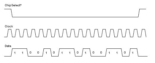
As we analyze a protocol and think about its implementation in LabVIEW FPGA we need to identify the different signal lines used by the protocol and the purpose of each signal. The number of signal lines used by the protocol will determine how many hardware resources we need to configure in the LabVIEW project and how many digital lines we will be using in the LabVIEW diagram. The following timing diagram (figure 1), showing the SPI (Serial Peripheral Interface) protocol, illustrates the use of three signal lines that we need to manage in the implementation of this protocol.
Figure 1: Simple timing diagram of the SPI protocol with one data line
As we start the implementation we realize that to convert the timing diagram into the corresponding LabVIEW FPGA code, we are concerned with two things - turning digital lines on and off and waiting the appropriate amount of time between setting the state of the different digital lines. In applications where we are reading a digital protocol we are concerned with reading the state of digital lines and noting the amount of time between any transitions on each signal line. Typically outputting a digital protocol is easier to implement and so we will address this case first.
One of the next criteria that we use to classify a protocol is the clock source used by the protocol. The two main categories are synchronous and asynchronous protocols. Synchronous protocols include a specific timing signal in the protocol, while asynchronous protocols are timed using a defined bit rate.
A typical example of a synchronous protocol is the SPI protocol shown in the timing diagram above. The protocol includes a dedicated clock signal allowing any receiver to use the clock line as the timebase to read or write the data line. Probably the best known asynchronous protocol is the serial (RS-232) bus used on many PCs. When using the serial bus we specify the baud rate (bits per second) of the device that we are communication with. The baud rate is used by the sender and receiver to update or read the data signal at the same rate. Because the time source will not be exactly the same on both ends of the communication, asynchronous communication data packets are limited in length to avoid bit misalignment. Asynchronous communication needs to re-synchronize frequently to allow for slight timing differences. Synchronous communication protocols on the other hand can communicate continuously as they are synchronized on every data bit.
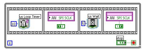
When we implement a clock signal as part of a synchronous protocol, the FPGA clock is used to determine the timebase of the protocol and update the clock signal accordingly.
Figure 2: LabVIEW FPGA diagram generating a 10 us (100 kHz) clock signal
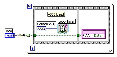
For an asynchronous protocol a separate clock signal is not generated, but the FPGA clock and defined baud rate is used to determine when to update or read the data signal(s).
Figure 3: LabVIEW FPGA diagram updating the data line at 4800 baud
(8333 FPGA clock cycles = 208.3 us = 1/4800 Hz)
Based on the rate specified by the clock signal or timing specification, data is encoded on the data signal or read from the data signal and then decoded. Encoding of data can be done in a number of different formats. The most common method is to represent the value of a data bit by one or several states of the data signal. This general class of encoding methods is called Pulse Code Modulation (PCM).
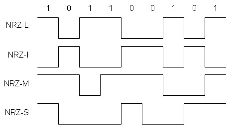
The subset of PCM methods in which the data bit is represented by a single state of the data signal are called Non-Return to Zero (NRZ). For example, a high data signal represents a '1' bit, while a low data signal represents a '0' bit. This method is called NRZ-L as the level of the data signal represents the data bit. In some protocols, such as RS-232, this logic is reversed where the high state represents '0', and the low state represents '1'. This is called NRZ-I (inverse). Additional NRZ subtypes are NRZ-M (mark) and NRZ-S (space) where the '1' data bit value is represented by a change in the data signal (NRZ-M) or a '0' is represented by a change of the data signal (NRZ-S).
Figure 4: NRZ (non-return to zero) encoding methods
Pulse code modulation includes another set of encoding schemes which combines the clock signal and data signal into one data line; each bit is represented by multiple states of the data signal. These are called bi-phase encoding and the common Manchester encoding scheme is one type of bi-phase encoding.
Other more advanced encoding schemes include different forms of pulse width encoding. The commonly used pulse width modulation (PWM) scheme converts an analog value directly into the varying pulse width of a constant frequency pulse train. Other forms of pulse width encoding use two different pulse width to represent a '0' and '1' bit in a traditional bit sequence.
Now that we have a basic nomenclature to describe common protocols we can look at how to implement protocols in LabVIEW FPGA. To implement a protocol in LabVIEW FPGA we typically start by walking through the timing diagram and converting the changes of state of the different signal lines and the timing between these changes into the corresponding LabVIEW functions and structures. Each change of state of a digital line is implemented using the FPGA I/O node and the timing is implemented using the LabVIEW FPGA timing functions (Loop Timer and Wait). Steps in the timing diagram that are repeated a number of times are implemented using the For or While Loop. For more extensive protocols groups of functions and structures may be encapsulated in subVI to allow code reuse and make the code more modular and manageable.
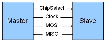
As our first example we implement the SPI timing diagram shown above in Figure 1 above. Communication using the SPI protocol consists of packets of data sent between two devices. In SPI communication there is a master device which controls the ChipSelect signal and the Clock signal. There may be one or more slave devices with dedicated ChipSelect signal line from the master to each slave and a common data line for all devices. If the application includes communication in both directions between master and slave(s), commonly two data lines are used; these are labeled Master Out Slave In (MOSI) and Master In Slave Out (MISO). In our example we will only focus on one data line.
Figure 5: Wiring diagram for SPI communication between two devices
Packet transfers are always initiated by the master device by asserting the ChipSelect line of the slave device being addressed. Commonly the ChipSelect line is active low so that it remains in a high state when the system is idle and is pulled low by the master to start a transmission. Following the assertion of the ChipSelect signal the master will update the data line and then toggle the clock line to transfer each data bit to the slave. The content of the data packet is application specific and left to the definition of the developer and device designer.
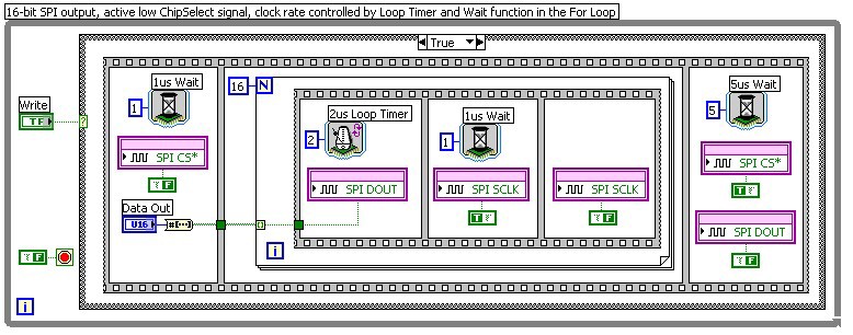
In the corresponding LabVIEW FPGA diagram (see figure 6 below) each data transfer is initiated by setting the 'Write' Boolean control. This causes the execution of the True case. Initially the ChipSelect line (SPI CS*) is asserted by driving the digital output low. At the same time the data value 'Data Out' is converted into the corresponding sequence of bits (Boolean array). The one microsecond (1us) wait function provides some time for the slave device to be ready for the following data bits. Then a sequence of updating the data line and toggling the clock line is repeated 16 times in the For loop. Each bit from the Boolean array is output to the data line (SPI DOUT), followed by the clock line (SPI SCLK) being set first high then low. The Loop Timer function allows the loop to run at 2 us intervals, while the Wait function controls the length of the high phase of the clock signal to be 1 us, generating a 500 kHz 50% duty cycle clock signal. After all 16 bits have been generated, the Chip Select and data lines are returned to their idle state and 5us minimum idle time Wait function is inserted. At this point the FPGA is ready for the next Write command.
Figure 6: LabVIEW FPGA diagram of a simple SPI output implementation
Based on the specification of the SPI devices being used and the application, any of the communication parameters (e.g. number of data bits to be transferred, frequency of the clock signal, etc. can be adjusted on the diagram or can be controlled dynamically using a control on the front panel of the LabVIEW FPGA VI.
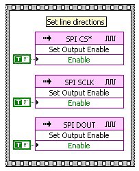
If necessary the direction of each of the digital lines used in the application can be set programmatically using the Set Output Enable FPGA I/O Method Node (see figure 7).
Figure 7: LabVIEW FPGA initialization of digital lines
Implementing the input portion of a protocol can present a few unique challenges as the code needs to be more flexible in detecting and processing the protocol. Rather than updating the digital output lines and inserting the appropriate delays, the code is monitoring the state of different digital lines and if necessary measuring time between specific transitions on the signal lines.
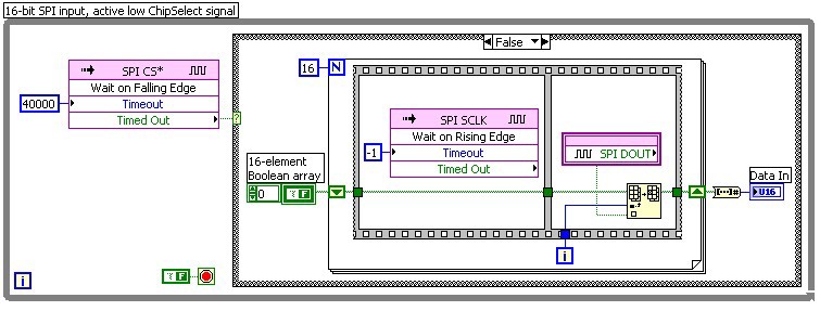
The following example shows a basic SPI input implementation, corresponding to the previous SPI output example. While in the Idle state the FPGA is monitoring the ChipSelect line and is detecting any falling edges. In response to a falling edge, it starts to monitor the clock line. For each of 16 rising edges of the clock signal, the FPGA reads the data signal and stores the bit value in a pre-allocated Boolean array. At the end of the data packet, after 16 clock cycles, the Boolean array is converted to an integer data value and made available on the front panel of the VI.
Figure 8: LabVIEW FPGA diagram of a simple SPI input implementation
Due to the nature of the SPI protocol this example does not need to make any time measurements as all timing is directly controlled by edges in the protocol.
In this section we address a number of additional topics to consider while developing a digital communication protocol using LabVIEW FPGA.
In the previous SPI examples each signal line is only driven by a single device. However, in many protocols signal lines may be driven or controlled by more than one device depending on the state of the bus or communication. This allows more than device to initiate transmission on the bus or to use the same data line to send and receive data. Typically this is achieved using an open-collector/open-drain circuit. In this configuration a device can only drive or pull a signal line low, but will let the signal line float when it wants to set the line high or not drive the line. In addition to each device that is connected to a signal line, the signal line also has a pull-up resistor to a set voltage to establish the high voltage of the line if none of the connected device are driving the signal low. Using this setup any device can drive the line low without creating a voltage contention between different devices. Such signals are typically defined to be active-low meaning that the line is in a high state when the bus is idle and a device will assert the signal by pulling the line low. Active-low signals are often indicated by a bar across the signal name or an asterisk after the signal name as in the case of the ChipSelect* (SPI CS*) signal used in the earlier examples.
To implement an open-collector signal in LabVIEW FPGA we use the ability to control the direction of the digital line to switch between driving a line low and letting it float. In LabVIEW FPGA the I/O Method Node is used to enable or disable a digital output line. While a line is disabled the FPGA does not drive the digital line and allows it to float high. To drive the line low when it is enabled, we set the Output Data to False. Output Data is a software register which maintains its value regardless whether the line is set to drive or float the line.
The following figures show an example of an open-collector configuration in LabVIEW FPGA for the I2C (Inter-Integrated Circuit) protocol. I2C is used in similar applications as SPI to communicate with different types of integrated circuits such as EEPROMs, ADC, DAC, etc. The I2C bus only has two signal lines, clock and data, and each is an open-collector line. To select the proper receiver for a communication the sender first transmits a unique device address which specifies the receiving device.
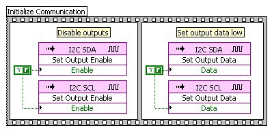
To initialize the VI for open-collector communication the two signal lines (SCL and SDA) are disabled to put the bus into the idle state. The Output Data for each signal is set to False. From this point on, the state of each line is controlled using the Set Output Enable method to enable the line and drive it low or to disable it and let it float high.
Figure 9: Configure two digital lines for open-collector communication
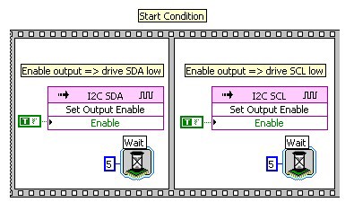
To initiate a transmission on the I2C bus, the sender transmits a start condition by driving the data line (SDA) low followed by driving the clock line (SCL) low.
Figure 10: Implement the I2C Start condition on the bus
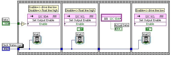
To transmit a data bit on the I2C bus (see figure 11), the sender updates the data line (1st frame), and then toggles the clock line high (2nd frame) and low (4th frame).
In the I2C protocol after each data byte (8 bits) is transferred, an extra clock cycle is inserted into the communication to allow the receiving device to acknowledge the successful reception of the previous byte. For this purpose the receiver pulls the data line low during the 9th clock cycle. On the sender side in our example this is implemented by sending a high data bit and checking the actual state of the data line (3rd frame) during the clock cycle. Even though the sender is letting the data line float high, the actual data value should be low as the receiver is pulling the data line low to acknowledge the last data byte.
Figure 11: Transmit a data bit on the I2C bus
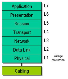
The OSI (Open Systems Interconnection) reference model is a representation of the different logical layers of a communication protocol including the application that is using the communication protocol. It is used to better define and understand the different aspects of a protocol and network.
Figure 12: OSI Reference Model
Layer 1 is the physical layer dealing with electrical and mechanical details providing the ability to send data across a carrier. Simple asynchronous packets operate at this level.
Layer 2 provides basic definition of bit and byte level data as well as modulation beyond NRZ and synchronization.
The next couple of layers deal with addressing, definition of data packets, error checking, etc.
As we can see from our examples the FPGA operates at the L1 Physical Layer interfacing directly to the each of the digital input and output lines at the electrical level. This means that we, as developers of a digital communication protocol in LabVIEW FPGA, are responsible for all layers of the reference model in regards to the protocol and application. For many simpler protocols this will only require a bit more programming than what we have done so far, to add an interface on top of the protocol layer to allow the application to interact with the FPGA and use the protocol. However, for more advanced protocols we may need significantly more programming to provide these intermediate protocol layers, such as bus level error detection and handling, packet building and parsing, handling different types of packets, etc.
As we have seen, timing plays a very important role in developing a protocol implementation. Data and clock lines need to be updated at precise intervals. While decoding a protocol it is important to accurately measure these same intervals. It is important to keep the timing behaviour of the FPGA in mind when we develop communication protocols to ensure that our implementation will meet the requirements and specifications of the protocol.
The FPGA operates on a base clock frequency and all timing functions are based on the same clock rate. For LabVIEW FPGA the default FPGA clock frequency is 40 MHz, so that each clock cycle and unit of time is 25 nanoseconds (ns). In LabVIEW FPGA we can specify time intervals for the timing functions in units of milliseconds, microseconds, and ticks. Each tick corresponds to one clock cycle or 25 ns. This means the highest resolution we have for specifying any delay or loop iteration time is 25 ns. While this sounds very accurate, when we take the inverse and determine the possible frequencies that we can generate we see the effect it has at higher rates.
To generate an update rate of 1 MHz for a digital line we can use a Loop Timer function set for 40 ticks.
1 MHz => 1 us = 1000 ns
1000 ns / 25 ns per tick = 40 ticks
What if we want an update rate of 1.25 MHz?
1.25 MHz =>0.8 us = 800 ns
800 ns / 25 ns per tick = 32 ticks
For 1.25 MHz we use a delay of 32 ticks. What if we want an update rate of 1.1 MHz?
1.1 MHz => 0.9091 us = 909.1 ns
909.1 ns / 25 ns per tick = 36.36 ticks
Since we can not choose specific partial clock cycles we would have to choose 36 clock cycles which is a delay of 900 ns and corresponds to a frequency of 1.111 MHz. The next lower frequency we could use is 37 ticks or 1.081 MHz. So we see that using the 40 MHz FPGA clock we can update the digital lines at 1.081 MHz or 1.111 MHz, but not in between.
Using the FPGA properties and clock resources in the LabVIEW project we have the option of changing the FPGA base clock frequency to 80 or 120 MHz. This will operate the FPGA at a higher frequency and improve the timing resolution of the timing functions. However, the higher clock frequency will also reduce the amount of complexity that can be used in the FPGA VI diagram and compiled successfully for the FPGA.
When planning to implement a timed protocol you need to determine if the timing resolution of the FPGA is adequate for the needs of the protocol and application. This is especially important for the timing required to generate a protocol as the previous calculations have shown. For reading and decoding protocols it is often adequate to be able to read the signal lines at a higher rate than the highest update rate of the protocol. We should be able to sample the signals at least twice as fast as the update rate to be safe.
If we need to make time measurements on an input signal to decode the data contained in the protocol then we need to make additional calculations to determine the timing resolution required to accurately decode the protocol.
State machines can be a useful technique to implement the encoding or decoding of a digital communication protocol. In LabVIEW state machines can be easily implemented using the While loop and a Case structure to represent each of the different states.
The state machine helps in the development of communication protocols as it naturally breaks down the timing diagram into separate steps and we can convert each into a separate state in the LabVIEW FPGA diagram. This isolates each program step and reduces the programming complexity in any one part of the implementation. In addition it simplifies generic operations such as error and exception handling by allowing us to jump from anywhere in the protocol execution to special error handling states. Sometimes protocol specifications are written in term of a state machine, which you can then directly translate into a LabVIEW state diagram.
For the SPI timing diagram in figure 1 the following steps are a possible way to break down the timing diagram into a state machine.
We notice that there are five unique steps, though some of them are repeated for each data bit. Originally we implemented these repeating steps in a For loop. In the state machine we create a unique state for each of these five steps and then cycle through them. For the three repeating steps that update data line and toggle the clock line, we configure the state machine to repeat this sequence 16 times before proceeding to the last step. In the LabVIEW state machine this is implemented using a counter in a shift register of the While loop.
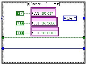
Another advantage of the state machine architecture is that it allows us to implement a protocol implementation inside a LabVIEW FPGA Single Cycle Timed Loop (SCTL). The SCTL provides faster execution of the LV FPGA diagram, allowing each cycle of the loop to execute in one clock cycle. This enables us to update a signal line at the FPGA base clock frequency. The SCTL also optimizes the code generation so that the code on the FPGA is more efficient and uses less FPGA real estate. However, there are several restrictions on the code implemented inside of a SCTL. For example we can only access each of the signal lines one time per SCTL iteration. Therefore we need to define the states of our state machine such that we only read or update each signal lines once per state.
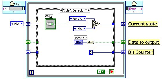
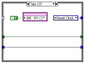
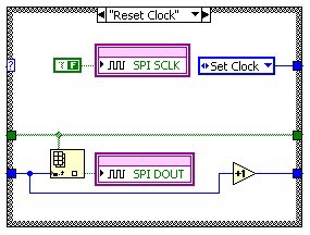
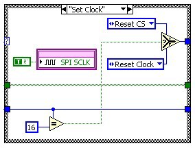
The following diagrams (figure 13) show the implementation of the SPI output protocol using a state machine inside of a SCTL. The Idle state waits for the Write command to start the output of the next data packet. It also converts the data value into a Boolean array for the output operation. The next step Set CS asserts the ChipSelect line. Then we start outputting the data bits. In Reset Clock we update the data line with the next bit value and reset the clock signal. In Set Clock we set the clock signal which triggers the receiver to read the data signal. In this pair of states we increment a counter in a shift register, which selects the proper data value from the Boolean array to send to the data line. After we output the 16th bit, we transition into the Reset CS state which resets all of the signal lines into the bus idle state. From there we go back to the Idle state and wait for the next Write command.
Figure 13: Implementation of SPI Output in a Single Cycle Timed Loop
Bi-phase encoding or modulation is a very common type of data encoding used in many different protocols. It combines the data signal and clock signal into one signal line, reducing the cabling needs and significantly improving data integrity over longer cabling distances.