Pulse Width Modulation Example DAQ Personality
Overview
Download the Pulse Width Modulation Example Personality.
Contents
LabVIEW FPGA Personality
The NI LabVIEW FPGA code is the portion of this code embedded on the R Series board. The code defines the FPGA in the same way an ASIC defines a multifunction DAQ board. It was written with LabVIEW FPGA and compiled into a bitfile. It is in its finalized form and does not require you to use the LabVIEW FPGA Module. However, you do need LabVIEW FPGA to customize this code.
This LabVIEW FPGA personality implements the single-cycle Timed Loop architecture, with each loop dedicated to a specific DIO line. See Figure 1 for a look at the block diagram for the LabVIEW FPGA code.
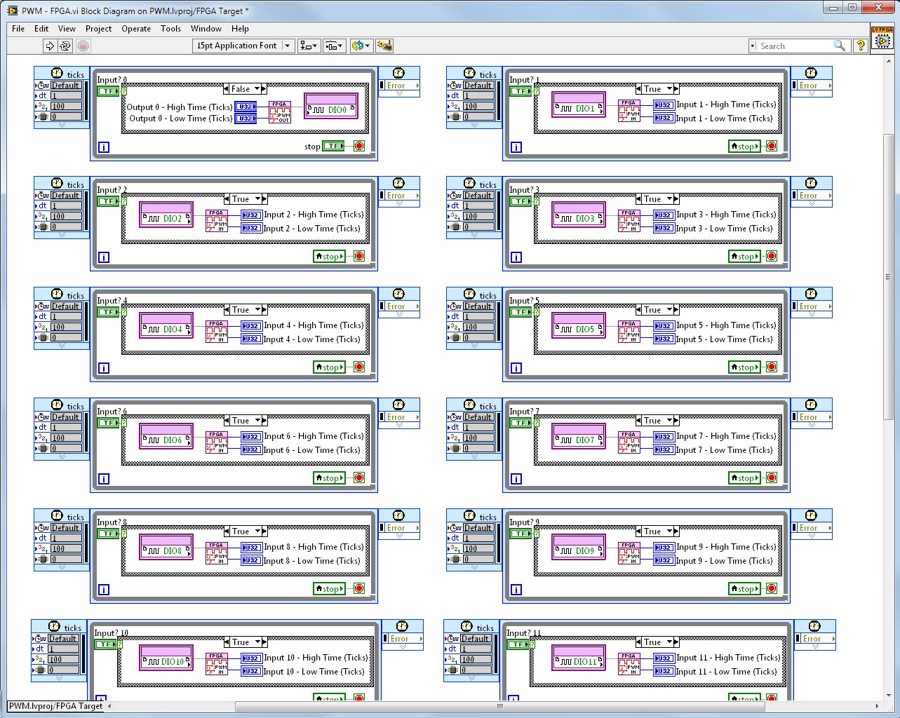
Figure 1. Block Diagram of the LabVIEW FPGA Code
PWM
Each single-cycle Timed Loop on the block diagram is dedicated to a particular DIO line and has the flexibility to perform PWM output or input. This functionality is defined by a simple Case structure and Boolean control. If the Boolean is set to a false value, the DIO line is used for PWM output. If the Boolean is set to a true value, the DIO line is used for PWM input. These two cases are shown in Figure 2 for DIO line 0.
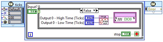
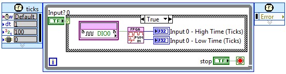
Figure 2. Single-Cycle Timed Loop Dedicated to DIO Line 0 (Both Cases)
PWM Input
For PWM input, a digital line is monitored at the rate of the FPGA clock (40 MHz in this case). The FPGA code counts the number of ticks (also known as clock pulses) that occur during both the low time and high time of the incoming signal. Those values are stored on the FPGA in the Low Period and High Period numeric indicators. These values can then be read by the host VI, which resides on the user’s computer. This is discussed in more detail in the upcoming sections.
See the PWM input logic in Figure 3.
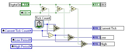
Figure 3. PWM Input Logic (Contained in a subVI)
PWM Output
For PWM output, the FPGA code is also run at the rate of the FPGA clock. The user provides the FPGA with the number of ticks desired for a high time and low time. The FPGA will output and sustain high or low for the duration of ticks desired.
See Figure 4 for the PWM output logic.
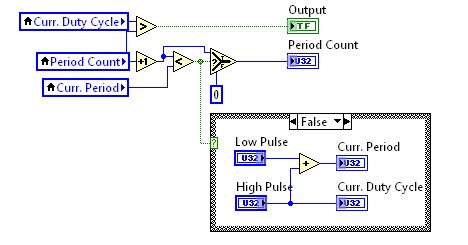
Figure 4. PWM Output Logic (Contained in a subVI)
Digital IO
The LabVIEW FPGA architecture makes it simple to add additional loops in parallel without affecting other parts of the FPGA application. For this reason, the LabVIEW FPGA code also takes advantage of the remaining DIO lines by configuring all of Connector 1 as static digital outputs and all of Connector 2 as static digital inputs. See this FPGA code in Figure 5.
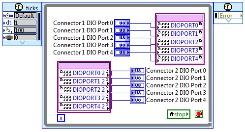
Figure 5. Static DIO Logic
LabVIEW Host Personality
The LabVIEW host code acts as the user interface used to communicate with the FPGA. The host code interacts directly with the FPGA code by updating controls and reading from indicators on the front panel of the FPGA code. This functionality is supported by the NI-RIO driver.
This example personality consists of three main steps:
1. Open a reference to the FPGA bitfile on the R Series target.
2. Use a Read/Write Node to update controls and indicators on the FPGA front panel.
3. Close the reference to the FPGA bitfile.
Block Diagram
See the example host block diagram in Figure 6.
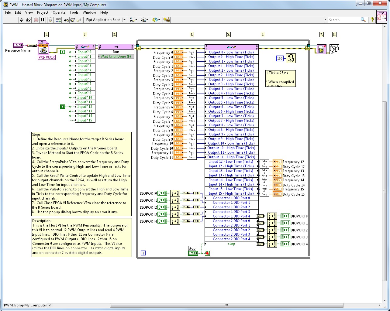
Figure 6. Block Diagram of the LabVIEW Host Code
These three main steps describe the overall setup of the host VI. This host code is a little more complex because of conversions that must take place prior to writing to a control. The following sections explain these three main steps in more detail.
1. Open Reference to Target FPGA
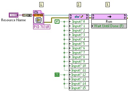
Figure 7. First Part of the Host Code
The first part of the code is the initialization stage. In this part, the resource name for the target R Series board is passed to the Open FPGA VI Reference. This function opens a reference to the board that can be used by any subsequent functions or subVIs that communicate with the FPGA. The reference is then passed to the Read/Write Node and the digital lines are initialized to function as an output or input. Finally, the Invoke Method Node is used to start the FPGA code on the R Series board.
2. Read FPGA Indicators and Write to FPGA Controls
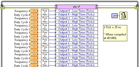
Figure 8. Middle Part of the Host Code
The middle part of the code consumes the majority of the execution time for this host VI. This part of the code consists of a While Loop with a Read/Write Node inside of it. The Read/Write Node gives users the ability to write to controls and read from indicators on the front panel of the FPGA code. In Figure 8, each input to the node is a control in the FPGA code.
For example, Output 0 – Low Time (Ticks) is the name of a control in the FPGA code. This particular control defines how many ticks DIO line 0 will output a low value. That control paired with Output 0 – High Time (Ticks) defines a PWM output channel (the high time and low time correlate to a frequency and duty cycle). Refer to Figure 1 to see these controls being used on the FPGA.
While LabVIEW FPGA supports fixed-point and floating-point data types, integer data types are the most efficient to use when it comes to consuming FPGA resources. For this reason, the data type written to the FPGA code is an integer (in this case it is a U32) and any division necessary is done on the host. The intermediate subVI, FreqtoPulse, converts the desired frequency and duty cycle for a PWM output channel to a low time and high time represented in ticks.
The While Loop executes at a rate defined by the Wait Until Next ms Multiple function. In this case, the user has defined the wait as 100 ms. This means that the While Loop executes every 100 ms, or at a rate of 10 Hz.
3. Close the FPGA Reference

Figure 9. Final Part of the Host Code
The final part of the host VI closes the reference to the R Series board. It also handles any errors that occurred during the execution of the host VI.
Front Panel
The host code front panel layout is in a quadrant form. PWM is on the left, DIO is on the right, outputs are on the top, and inputs are on the bottom. Figure 10 shows the front panel.
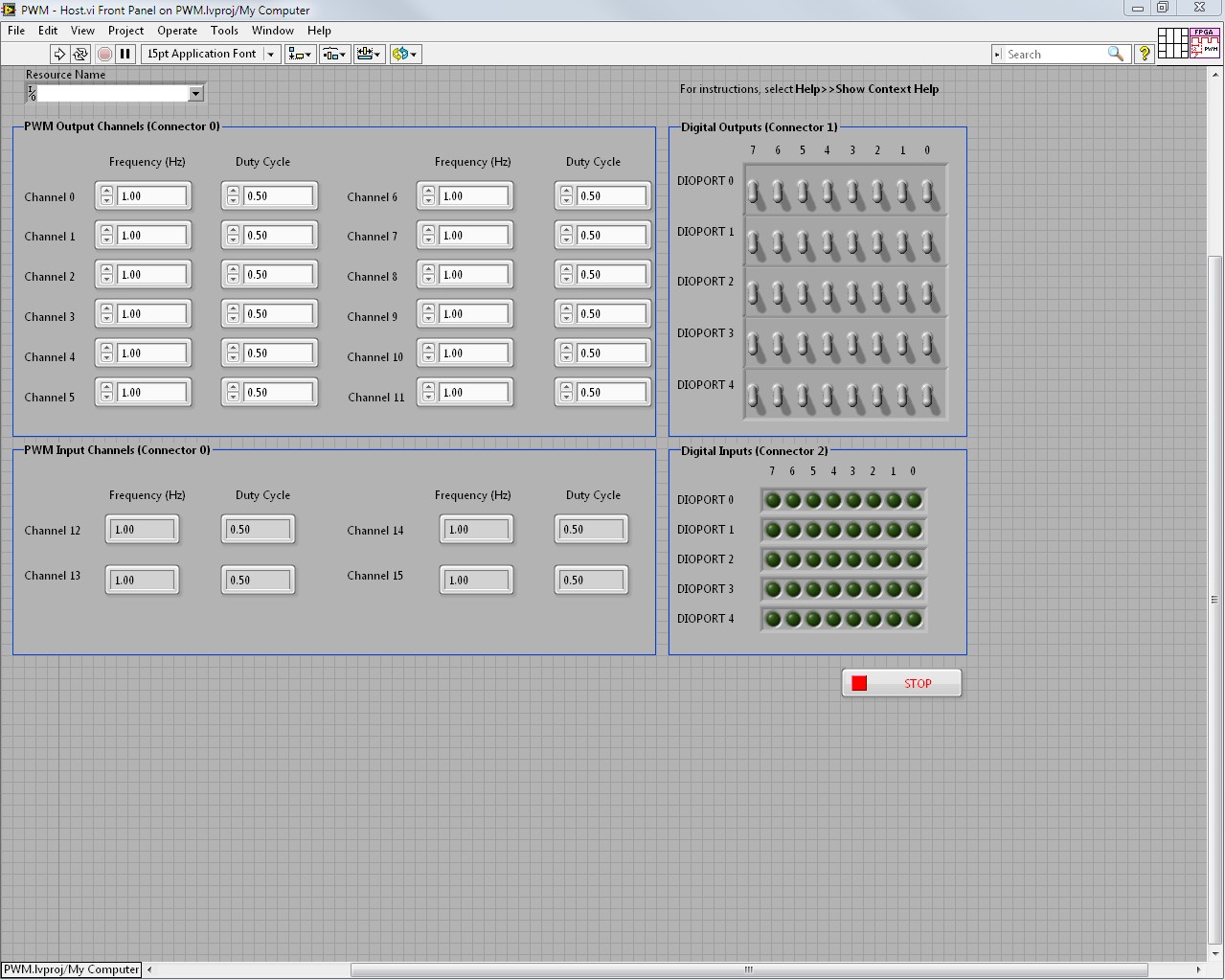
Figure 10. Front Panel of the LabVIEW Host Code
Conclusion
You can use this example personality for high-channel-count PWM. You do not need the LabVIEW FPGA Module to use this personality. However, you do need the module if you want to make any modifications to the FPGA code. The NI-RIO driver is the only driver necessary.